Method for making Nano microstructure based on constant height mode of atomic force microscope

An atomic force microscope and microstructure technology, which is applied in nanostructure manufacturing, nanotechnology, nanotechnology, etc., can solve problems such as limited size range, and achieve the effect of overcoming poor repeatability positioning accuracy, high repeatability positioning accuracy, and easy precision

Inactive Publication Date: 2007-07-25
HARBIN INST OF TECH
View PDF0 Cites 21 Cited by
  • Summary
  • Abstract
  • Description
  • Claims
  • Application Information

AI Technical Summary

Problems solved by technology

[0004] The purpose of the present invention is to provide a nano-microstructure processing method based on the constant height mode of the original force microscope, to overcom

Method used


Image

  • Method for making Nano microstructure based on constant height mode of atomic force microscope
  • Method for making Nano microstructure based on constant height mode of atomic force microscope
  • Method for making Nano microstructure based on constant height mode of atomic force microscope

Examples


specific Embodiment approach 1

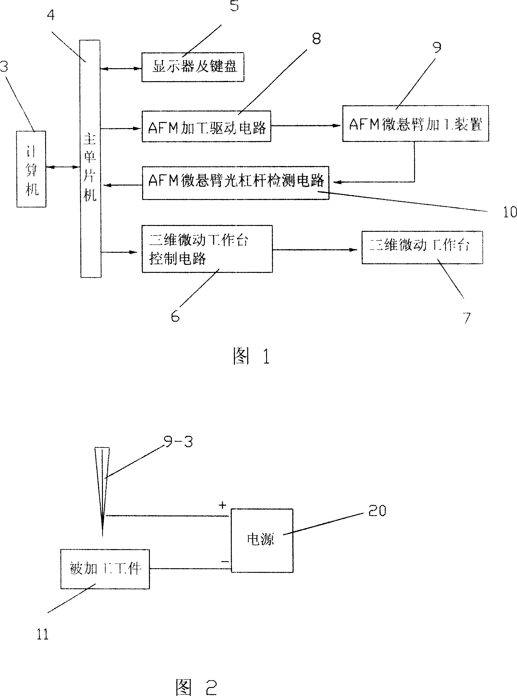
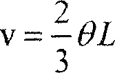
[0008] Specific Embodiment 1: The present embodiment will be specifically described below with reference to FIG. 1 , FIG. 3 and FIG. 4 . The system of this method consists of a computer 3, a main single-chip microcomputer 4, a display and a keyboard 5, a three-dimensional micro-motion workbench control circuit 6, a three-dimensional micro-motion workbench 7, an AFM processing drive circuit 8, an AFM micro-cantilever processing system 9 and an AFM micro-cantilever light beam. Composed of lever detection circuit 10, AFM microcantilever processing system 9 includes scanning pottery tube 9-1, cantilever 9-2, probe 9-3 and optical lever angle measuring device 9-4, and the communication port of computer 3 is connected to one of main single chip microcomputer 4 Communication port, another communication port of main single-chip microcomputer 4 connects the communication port of display and keyboard 5, an output end of main single-chip microcomputer 4 connects the input end of AFM proce...

specific Embodiment approach 2

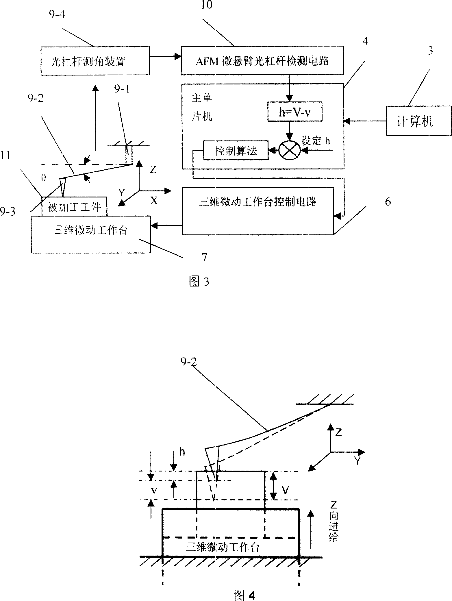
[0014] Specific Embodiment 2: The present embodiment will be specifically described below with reference to FIG. 2 . The difference between this embodiment and Embodiment 1 is that its system also includes a power supply 20, the positive and negative poles of the power supply 20 are respectively connected to the probe 9-3 and the workpiece 11 to be processed, and the voltage amplitude of the power supply 20 is less than 10V, which is continuous The pulse time is 500ms. This function is another function added to the scoring function. The probe 9-3 and the workpiece 11 to be processed apply a voltage signal set by the user, and the voltage signal is independently isolated from other parts of the system, which can realize the needle-tip-induced local oxidation processing and needle-tip-induced local modification processing of the workpiece 11 .


PUM


Abstract

A process based on the constant-height mode of atomic force microscope for preparing nano-class microstructure with controllable depth and large range of precise sizes features that 3D micro-motion bench and its control circuit is additionally used. The motion of said 3D micro-motion bench in height direction is driven by its control circuit to make the probe tip to prick into the surface of a workpiece to be processed. The deformation amount of cantilever caused by the reactive force received by said probe is detected by optical angular measurer and transmitted to single-chip computer. Said 3D bench is moving continuously in the height direction until the processed depth setting is equal to the difference between the motion amount of said 3D bench in height direction and said deformation amount of cantilever.

Description

technical field [0001] The invention relates to a processing method of a nanoscale microstructure. Background technique [0002] In 1982, Gerd Binnig and Heinrich Roher of IBM invented the first scanning tunneling microscope (STM), and in 1983 they successfully observed the Si(7×7) atomic distribution image on the Si(111) surface. Subsequently, scientists invented a series of nanoscale surface detection instruments using probes as tools on the basis of STM. In 1986, Gerd Binnig and others invented the atomic force microscope (AFM) on the basis of STM. It solves the problem that STM has high requirements on the environment and samples, and greatly broadens the scope of application. The invention of laser deformation detection technology in 1988 and the successful batch production of microprobes by Stanford University in the United States in 1989 further improved the stability of AFM and greatly promoted the application of AFM in various fields. In recent years, combined wi...

Claims


Application Information

Patent Timeline
IPC IPC(8): B82B3/00
Inventor 孙涛胡振江闫永达赵学森董申
Owner HARBIN INST OF TECH
Why Eureka
Try Eureka