
Solid-state imaging device and electronic endoscope using the same

A solid-state imaging device and solid-state imaging technology, which are applied in the field of electronic endoscopy and can solve the problems of increasing the thickness of the solid-state imaging device and the like

Inactive Publication Date: 2010-05-19
FUJIFILM CORP +1
View PDF6 Cites 11 Cited by
  • Summary
  • Abstract
  • Description
  • Claims
  • Application Information

AI Technical Summary

Problems solved by technology

For example, in Figure 9 In the case of the solid-state imaging device shown in , since the solid-state imaging element 104 is mounted in the package 201, the thickness of the entire solid-state imaging device becomes substantially larger by t1

Method used


Image

  • Solid-state imaging device and electronic endoscope using the same
  • Solid-state imaging device and electronic endoscope using the same
  • Solid-state imaging device and electronic endoscope using the same

Examples


no. 1 example

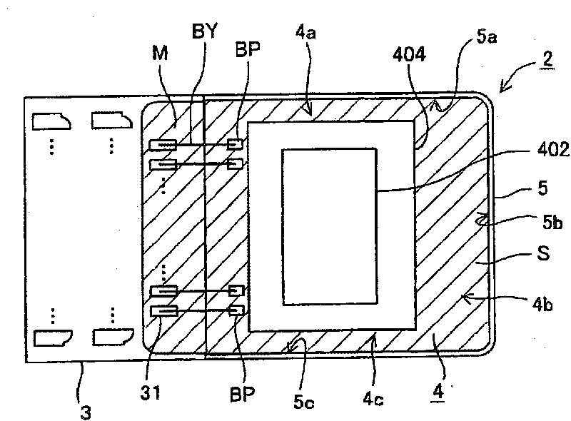
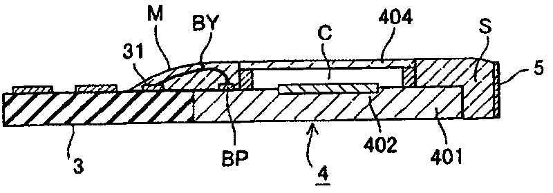
[0029] Such as Figure 1A with 1B As shown in , the solid-state imaging device 2 according to the first embodiment has a substrate 3 , a solid-state imaging element 4 , and a frame 5 . It should be noted that letter symbol M in the drawings indicates a sealing resin portion.

[0030] For these parts, the substrate 3 is formed of ceramics and has a substantially plate-like shape, and one end face of the substrate 3 ( Figure 1B The right end face in ), by using a suitable adhesive (such as UV adhesive) to fix with one end face of the solid-state imaging element 4 ( Figure 1B The left end face in ) integration.

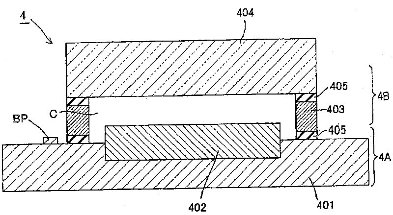
[0031] The solid-state imaging element 4 is constituted as a chip size package (CSP) type solid-state imaging element, and in terms of the overall configuration of the solid-state imaging element 4, as Figure 2A As shown in , the solid-state imaging element 4 has a solid-state imaging element substrate 4A and a cover glass 4B. Among these components, the solid-st...

no. 2 example

[0060] Figure 8 An electronic endoscope of a direct observation type provided with a solid-state imaging device according to a second embodiment of the present invention is shown. In this electronic endoscope, the solid-state imaging device 2 according to the first embodiment is installed inside the distal end portion 10 of the endoscope main body 1 .

[0061] The endoscope main body 1 is provided with: an observation channel 1A for observing an area to be observed through an objective lens 12, a prism 13, etc., from an observation window 11 opened on a distal end surface; and a treatment An instrument insertion channel 1B for performing various treatments by inserting an unillustrated therapeutic instrument through the forceps hole 14 from the forceps window 15 opened at the distal end face.

[0062] Therefore, according to this embodiment, when combined with Figure 9 When compared with the solid-state imaging device having the thickness of the prior art shown in , the sol...


PUM


Abstract

A solid-state imaging device comprises: a solid-state imaging element comprising a solid-state imaging element body; a first substrate one end face of which is bonded to and integrated with one end face of a solid-state imaging element substrate of the solid-state imaging element, the first substrate comprising on its one surface an electrode for establishing electrical contact with a bonding wireled from a pad provided on one surface of the solid-state imaging element, a frame that seals the solid-state imaging element so as to surround outer peripheral surfaces of the solid-state imaging element substrate excluding its the one end face; and a sealing resin portion that covers a region extending from a portion including the electrode on the one surface of the first substrate to a portionincluding the pad on the one surface of the solid-state imaging element.

Description

technical field [0001] The present invention relates to a solid-state imaging device and an electronic endoscope using the same, and more particularly, to a solid-state imaging device such as a chip size package (CSP) type having a microlens integrated on a chip and a solid-state imaging device having the same An electronic endoscope with a solid-state imaging device. Background technique [0002] Various electronic type endoscopic devices, which are inserted into body cavities and achieve effects such as observing the inside of the body cavity, have been proposed and developed for biomedical use. In addition, various solid-state imaging elements including charge-coupled devices (CCDs) are used in these electronic type endoscopic devices. [0003] In direct observation type cases, for example, as in Figure 9 As shown in , the known electronic type endoscopic equipment is configured such that a solid-state imaging element 104 is installed inside the distal end portion of th...

Claims


Application Information

Patent Timeline
Patent Type & Authority Patents(China)
IPC IPC(8): H01L27/148H01L23/00H01L23/10A61B1/04
CPCH04N5/2252H01L2224/49175H01L2224/48091A61B1/051H04N5/2253G02B23/2484H01L2224/45144H01L31/0203H01L2924/3025A61B1/018A61B1/05H01L27/14618H01L2224/05553H01L2924/16235H04N23/51H04N23/54H01L2924/00014H01L2924/00
Inventor 岛村均高桥一昭西田和弘
Owner FUJIFILM CORP
Learn More