Supercharge Your Innovation With Domain-Expert AI Agents!

Semiconductor device and manufacturing method for the same

一种制造方法、半导体的技术,应用在半导体/固态器件制造、半导体器件、半导体/固态器件零部件等方向,能够解决附着性差、附着性易受环境条件的影响、树脂膜易脱落等问题

Inactive Publication Date: 2007-08-15
SOCIONEXT INC
View PDF3 Cites 3 Cited by
  • Summary
  • Abstract
  • Description
  • Claims
  • Application Information

AI Technical Summary

Problems solved by technology

Therefore, there is a problem that the end of the resin film is likely to come off due to the poor adhesion between the interconnection and the resin film
The adhesion between the interconnect and the resin film is susceptible to environmental conditions, i.e. the resin film tends to fall off under the action of heat and stress
For example, when a semiconductor device is subjected to a high-low temperature cycle test as a reliability evaluation test, the opening of the resin film degrades to cause the resin film to peel off, which can sometimes lead to the peeling off of the interconnection

Method used


Image

  • Semiconductor device and manufacturing method for the same
  • Semiconductor device and manufacturing method for the same
  • Semiconductor device and manufacturing method for the same

Examples


example 1

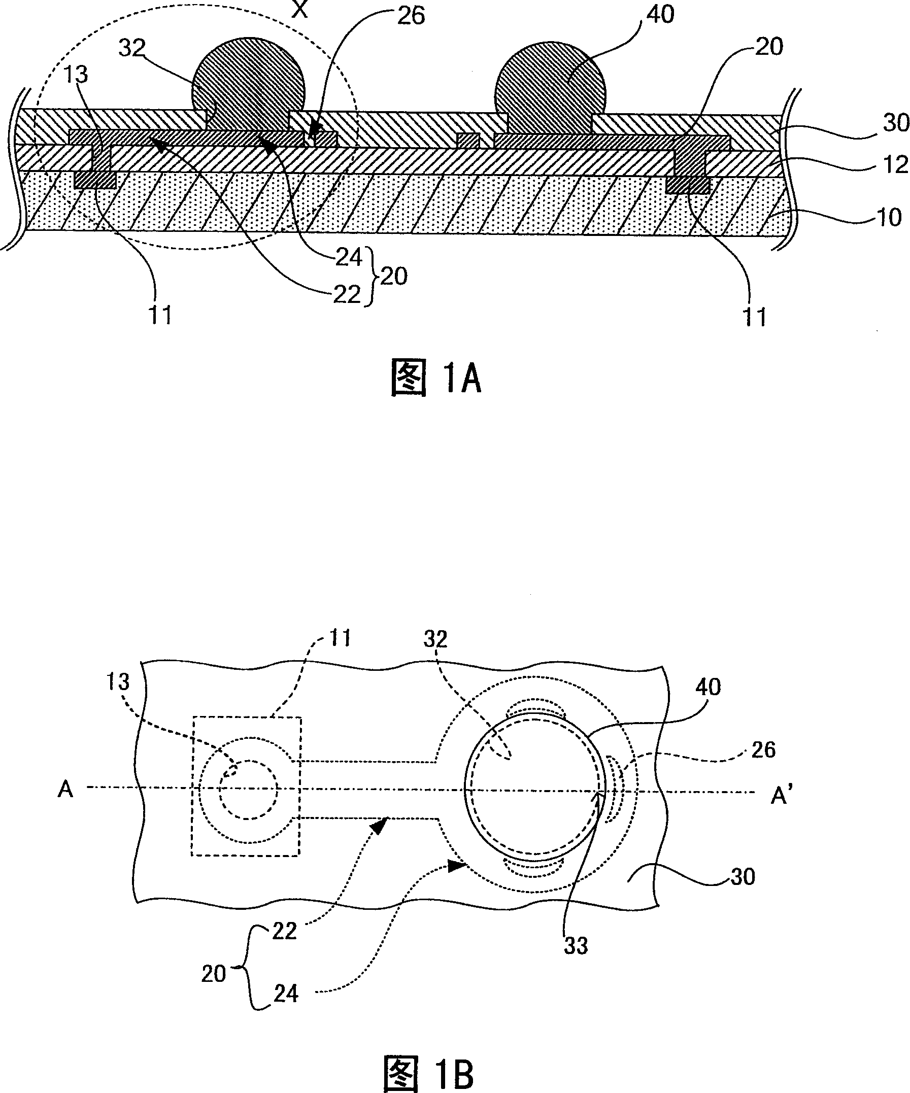
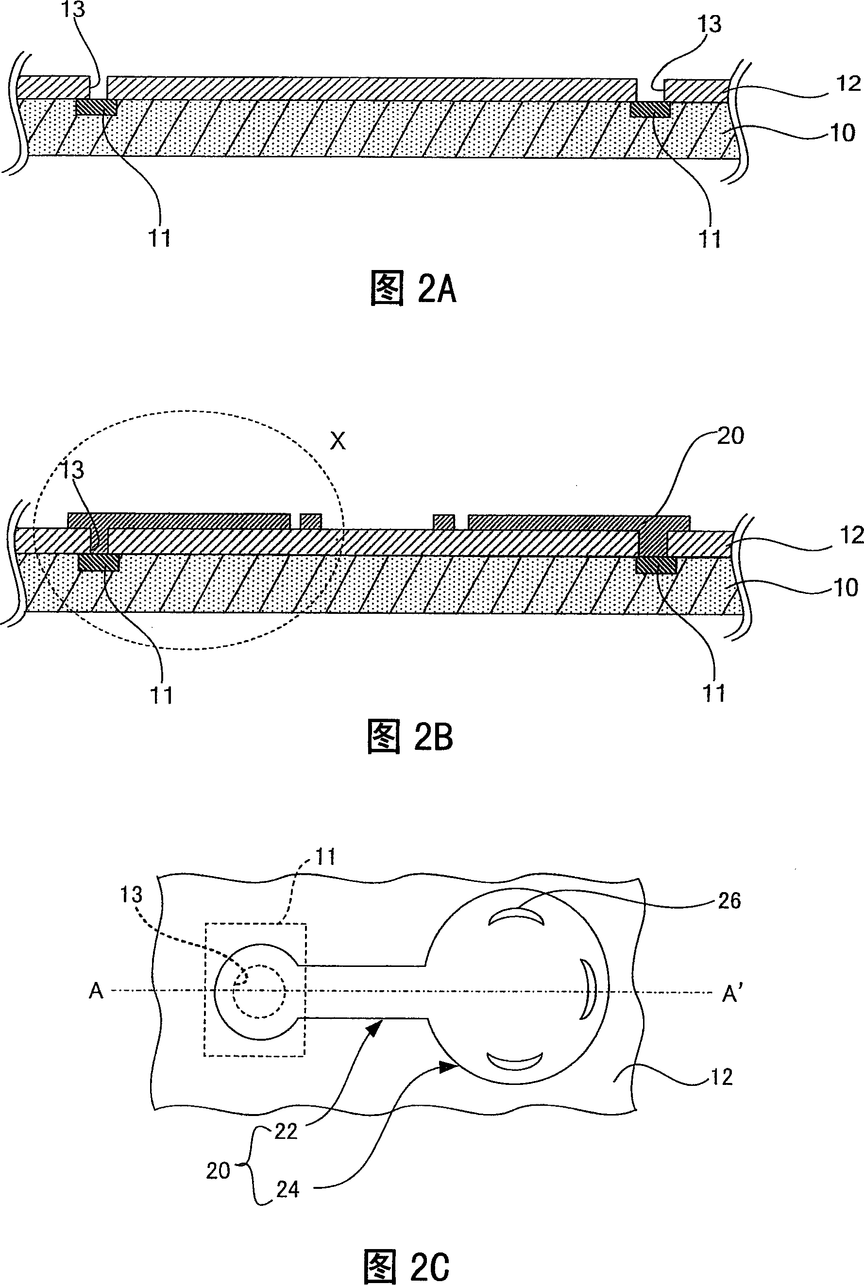
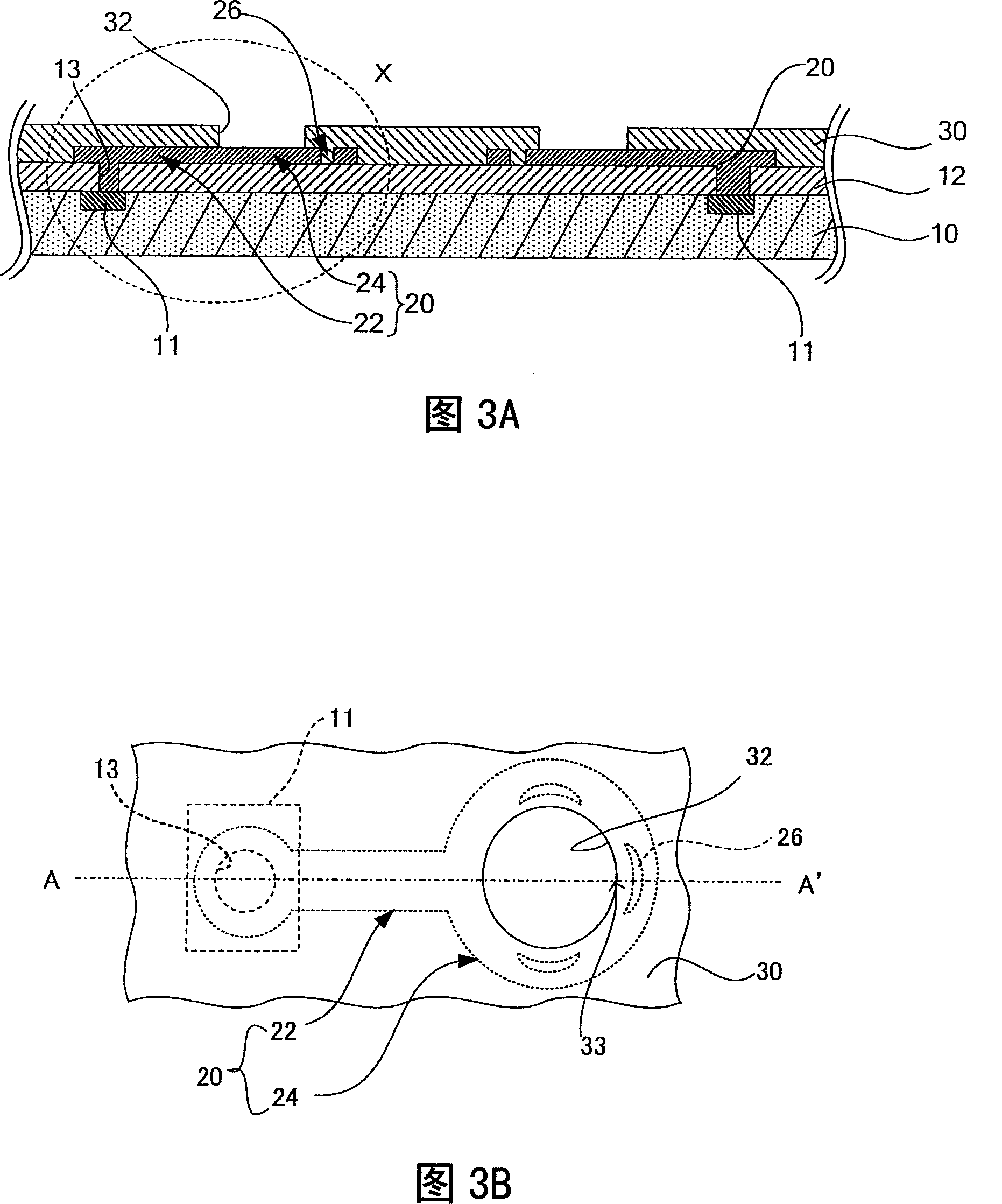
[0035] A first example of the semiconductor device of the present invention is shown in FIGS. 1A and 1B. FIG. 1A is a cross-sectional view along line A-A' of FIG. 1B , and FIG. 1B is a top view of a portion "X" surrounded by a dotted line in FIG. 1A .

[0036] In the semiconductor device shown in FIG. 1A, an insulating film 12 made of, for example, polyimide resin is formed on a silicon wafer 10 having an Al pad 11 serving as the above-mentioned semiconductor substrate. The insulating film 12 is provided in such a manner as to avoid the space above the Al pad 11 where the connection hole 13 is to be provided.

[0037] A conductive layer (or interconnection) 20 made of copper is provided on the surface of the insulating film 12 and fills the connection hole 13 . The A1 pad 11 and the conductive layer 20 are bonded together via the connection hole 13 . Conductive layer 20 is formed of interconnection portion 22 and pad portion 24 . As shown in FIG. 1B , three via holes 26 pen...

example 2

[0062]A second example of the semiconductor device of the present invention is shown in FIGS. 4A and 4B. In each drawing, the upper part shows a top view of the semiconductor device, and the lower part shows a cross-sectional view along line B-B' of the top view.

[0063] In the semiconductor device shown in FIG. 4A , there are provided four through holes 26 arranged at substantially equal distances from the end of the exposed opening (ie, the end 33 of the resin film opening 32 ), The exposure opening occurs over at least a portion of the pad portion 24 of the conductive layer 20, and the four via holes 26 are spaced apart from each other by substantially equal distances.

[0064] Note that, when the semiconductor device shown in FIG. 4A is manufactured, in the above-mentioned conductive layer forming step, four via holes 26 are formed in the conductive layer 20 in the following manner as viewed from above the horizontally divided silicon wafer 10: four vias The shapes of th...

example 3

[0066] A third example of the semiconductor device of the present invention is shown in FIG. 5 . FIG. 5 is a plan view of a pad portion of the semiconductor device showing the configuration of via holes provided on the pad portion.

[0067] As shown in FIG. 5 , in Example 3, eight via holes 27 penetrating the conductive layer 20 are provided. When viewed from above the horizontally divided silicon wafer 10, the eight through holes 27 have substantially the same circular shape, and their sizes are also substantially the same. In addition, the eight through holes 27 are arranged at substantially equal distances from the end of the exposure opening (or, the end 33 of the resin film opening 32 ) that appears over at least a part of the pad portion 24 of the conductive layer 20 . , and the eight through holes 27 are spaced from each other at substantially equal distances.

[0068] As described above, in Example 3, since the eight through holes 27 are symmetrical about the center ...


PUM


Abstract

To provide a semiconductor device with high performance and reliability, in which peeling off an interconnection layer caused due to peeling off of a resin film at a land part is suppressed and thus electrical break down is prevented, and an efficient method for manufacturing the semiconductor device. The semiconductor device includes a semiconductor substrate (e.g., a silicon wafer 10 ); an insulating film 12 formed on the semiconductor substrate 10; a conductive layer 20 formed on the insulating film 12, the conductive layer 20 formed of an interconnection part 22 and a land part 24 which connects the interconnection part 22 to an external terminal 40; and a resin film 30 covering the conductive layer 20, wherein the resin film 30 is in contact with the insulating film 12 at least at a part of the land part 24 by passing through the conductive layer 20.

Description

[0001] Cross References to Related Applications [0002] This application is based on and claims priority from prior Japanese Patent Application No. 2006-028850 filed on February 6, 2006, the entire contents of which are hereby incorporated by reference. technical field [0003] The present invention relates to a semiconductor device having high performance and high reliability, in which peeling of an interconnection layer due to peeling of a resin film at a pad portion is suppressed, and an efficient manufacturing method thereof is avoided, thereby avoiding electrical breakdown. Background technique [0004] In recent years, with the development trend of thinner and smaller electronic devices, people are trying to reduce the size of semiconductor devices and increase the packaging density of semiconductor devices. Against this background, wafer-level packaging has been proposed, which reduces the size by minimizing the size of a semiconductor device to be as close as possi...

Claims


Application Information

Patent Timeline
Patent Type & Authority Applications(China)
IPC IPC(8): H01L23/485H01L23/50H01L23/522H01L21/28H01L21/60H01L21/768
CPCH01L2924/014H01L2924/01023H01L24/05H01L2924/01029H01L24/13H01L2924/01005H01L2924/01004H01L2924/01082H01L2224/13099H01L2224/0231H01L2924/01078H01L2924/01013H01L23/3114H01L2924/01006H01L2924/01033H01L2224/0401H01L2924/15787H01L2224/05556H01L2924/00H01L21/3205H01L23/12
Inventor 爱场喜孝
Owner SOCIONEXT INC
Features
  • R&D
  • Intellectual Property
  • Life Sciences
  • Materials
  • Tech Scout
  • Unparalleled Data Quality
  • Higher Quality Content
  • 60% Fewer Hallucinations
Learn More