Field emission assisted microdischarge devices

A field emission and electrical device technology, applied in the direction of discharge tube/lamp parts, discharge tube, electrical components, etc., can solve the problems of limiting the length and diameter of carbon nanotubes, the surface number density of carbon nanotubes, etc.

Inactive Publication Date: 2007-08-15
THE BOARD OF TRUSTEES OF THE UNIV OF ILLINOIS
View PDF3 Cites 2 Cited by
  • Summary
  • Abstract
  • Description
  • Claims
  • Application Information

AI Technical Summary

Problems solved by technology

Electronic applications of carbon nanotubes usually rely only on field emission as a current source, which requires an electrode voltage of 150 V to 1 kV and limits the length and diameter of the carbon nanotubes and the surface number density of the carbon nanotubes in the array

Method used


Image

  • Field emission assisted microdischarge devices
  • Field emission assisted microdischarge devices
  • Field emission assisted microdischarge devices

Examples


Embodiment Construction

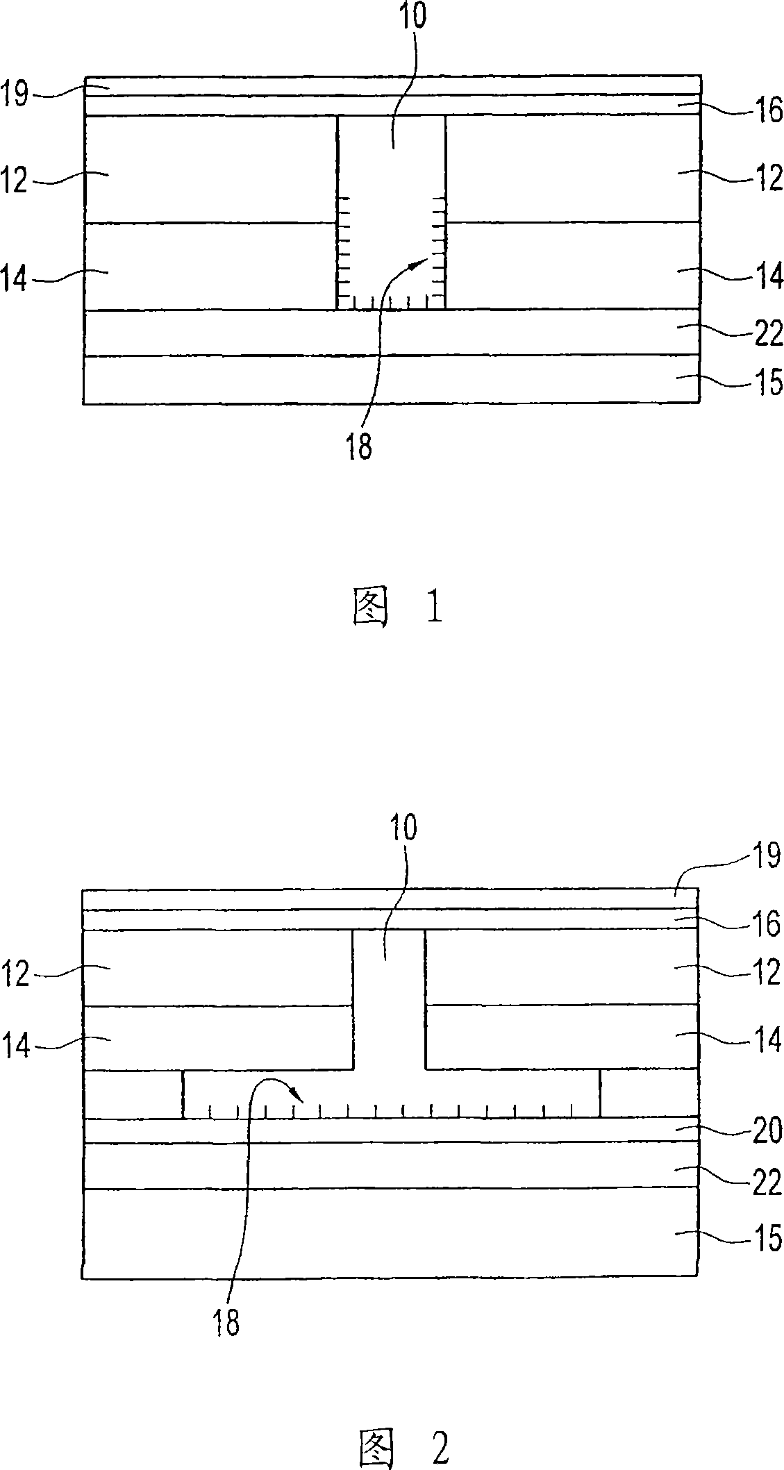
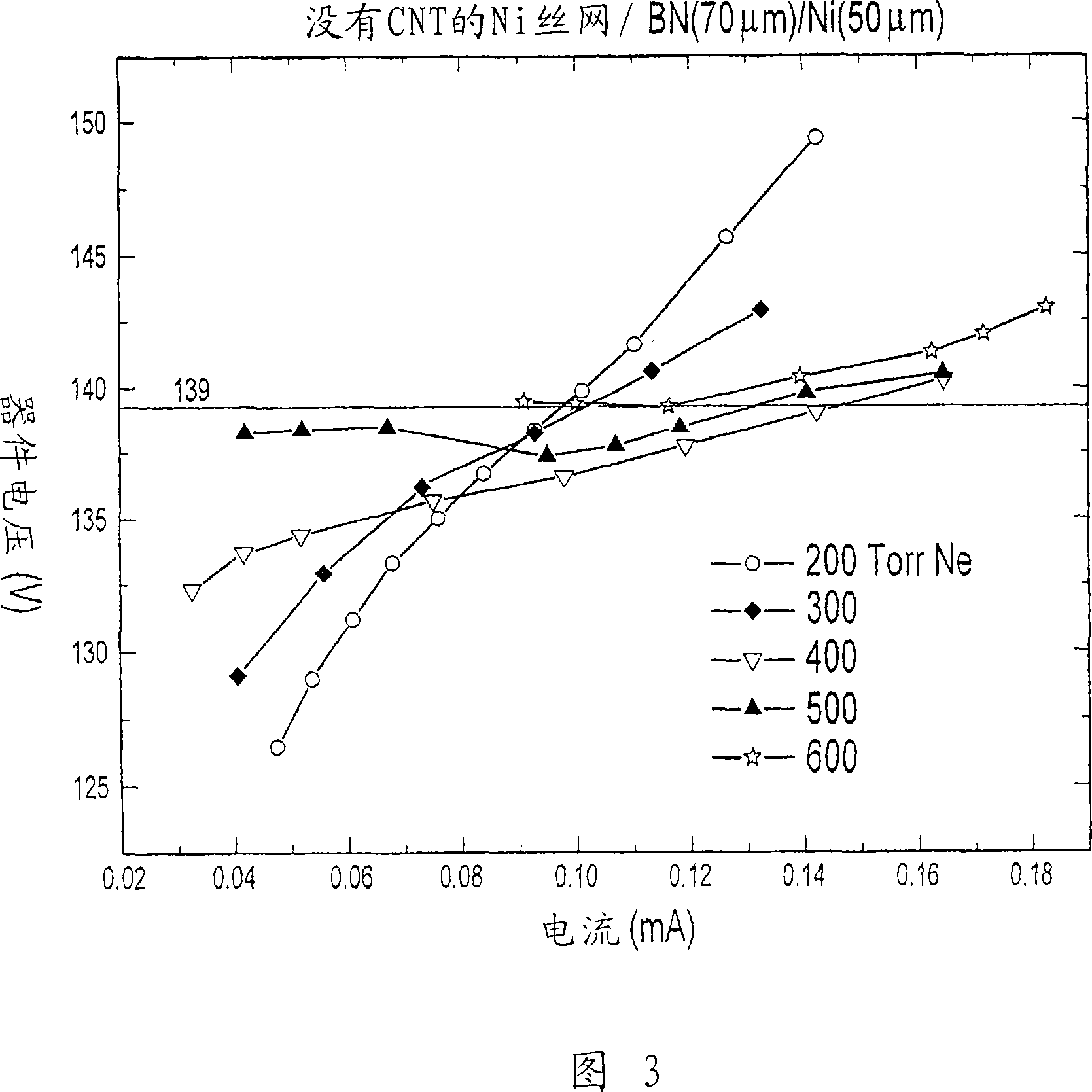
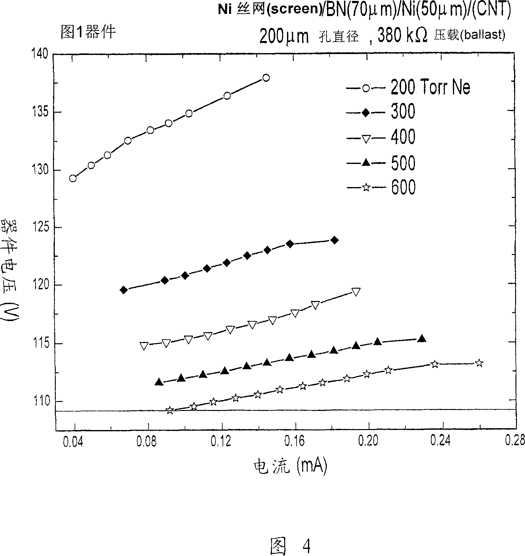
[0018] The present invention relates to a micro-discharge device with field emission nanostructure assisting work. Example embodiments of the present invention include microdischarge devices having field emission nanostructures integrated into the device and microdischarge devices having field emission nanostructures disposed near the cathode of the device. Exemplary methods of the present invention include the use of field emission nanostructures to assist in the operation of microdischarge devices. An exemplary array of the present invention includes a plurality of microdischarge devices, where each device (pixel) has a field emission nanostructure to assist in its operation.

[0019] The present invention is applicable to many different microdischarge devices, including those described in the US patents and US / PCT patent applications listed in the Background section. The invention will now be illustrated by a discussion of the preferred embodiment device. The skilled pers...


PUM


Abstract

Field emission nanostructures (18) assist operation of a microdischarge device. The field emission nanostructures are integrated into the microdischarge device(s) or are situated near an electrode (14, 16, 36, 38) of the microdischarge device(s). The field emission nanostructures reduce operating and ignition voltages compared to otherwise identical device lacking the field emission nanostructures, while also increasing the radiative output of the microdischarge device(s).

Description

technical field [0001] The field of the invention is microdischarge devices and arrays. Other fields of the invention include all fields using incoherent light and certain embodiments of the invention are also applicable to fields using coherent light. Examples of applications of devices of the present invention that produce incoherent emission include displays and more mundane lighting applications. Examples of applications of devices of the present invention that produce coherent emission include, for example, the fields of fiber optic communications, biomedical diagnostics, and environmental sensing. Background technique [0002] Microdischarge devices, also known as microplasma or microcavity discharge devices, have been developed as alternatives to other light emitting devices. Microdischarge devices have been disclosed in the following U.S. patents: 6,563,257, entitled Multilayer Ceramic Microdischarge Devices; 6,541,915, entitled High Voltage Arc Lamp Assisted Start...

Claims


Application Information

Patent Timeline
Patent Type & Authority Applications(China)
IPC IPC(8): H01J1/62H01J1/02
CPCB82Y10/00H01J2217/49H01J2201/30469H01J3/025H01J17/066H01J63/02H01J1/025B82Y40/00H01J1/304
Inventor 朴晟镇J·加里·伊登朴璟虎
Owner THE BOARD OF TRUSTEES OF THE UNIV OF ILLINOIS
Why Eureka
Try Eureka