A sonos memory device with optimized shallow trench isolation

A technology of shallow trenches and devices, which is applied in the manufacture of electric solid devices, semiconductor devices, semiconductor/solid devices, etc., can solve problems affecting the electronic characteristics of SONOS units, and achieve the effect of reducing thickness changes

Active Publication Date: 2007-08-15
NXP BV
View PDF1 Cites 8 Cited by
  • Summary
  • Abstract
  • Description
  • Claims
  • Application Information

AI Technical Summary

Problems solved by technology

However, in a SONOS memory cell, such thickness variation of the first silicon dioxide layer SD1 affects the electronic characteristics of the SONOS cell

Method used


Image

  • A sonos memory device with optimized shallow trench isolation
  • A sonos memory device with optimized shallow trench isolation
  • A sonos memory device with optimized shallow trench isolation

Examples


Embodiment Construction

[0037] For the purpose of illustrating the invention, preferred embodiments of the methods and devices of the invention are described below. It will be appreciated by those skilled in the art that other alternative and equivalent embodiments of the invention can be conceived and put into practice without departing from the scope of the invention, which is only defined by the appended claims.

[0038] Objects denoted by the same reference numerals refer to the same objects shown in the preceding figures.

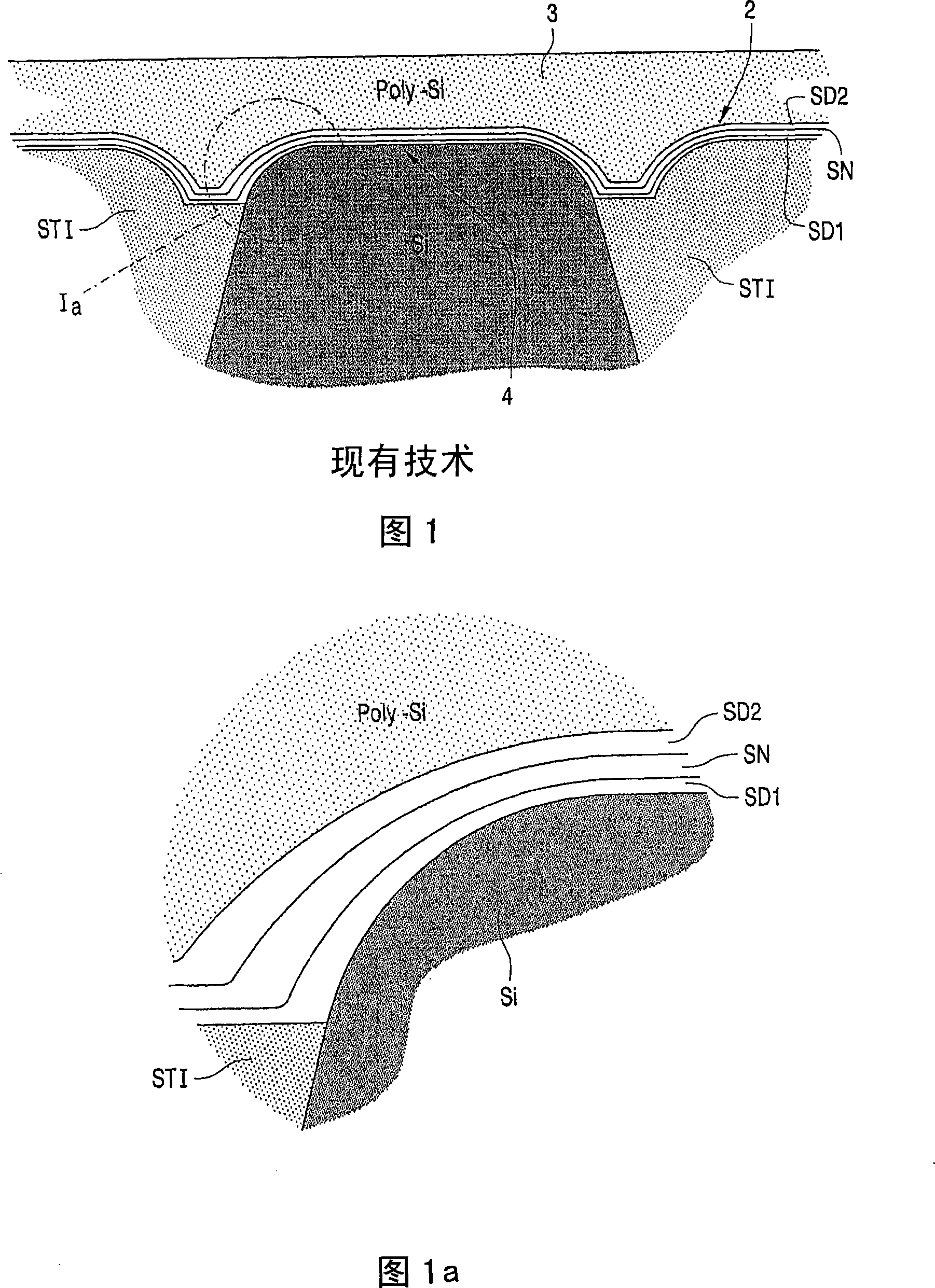
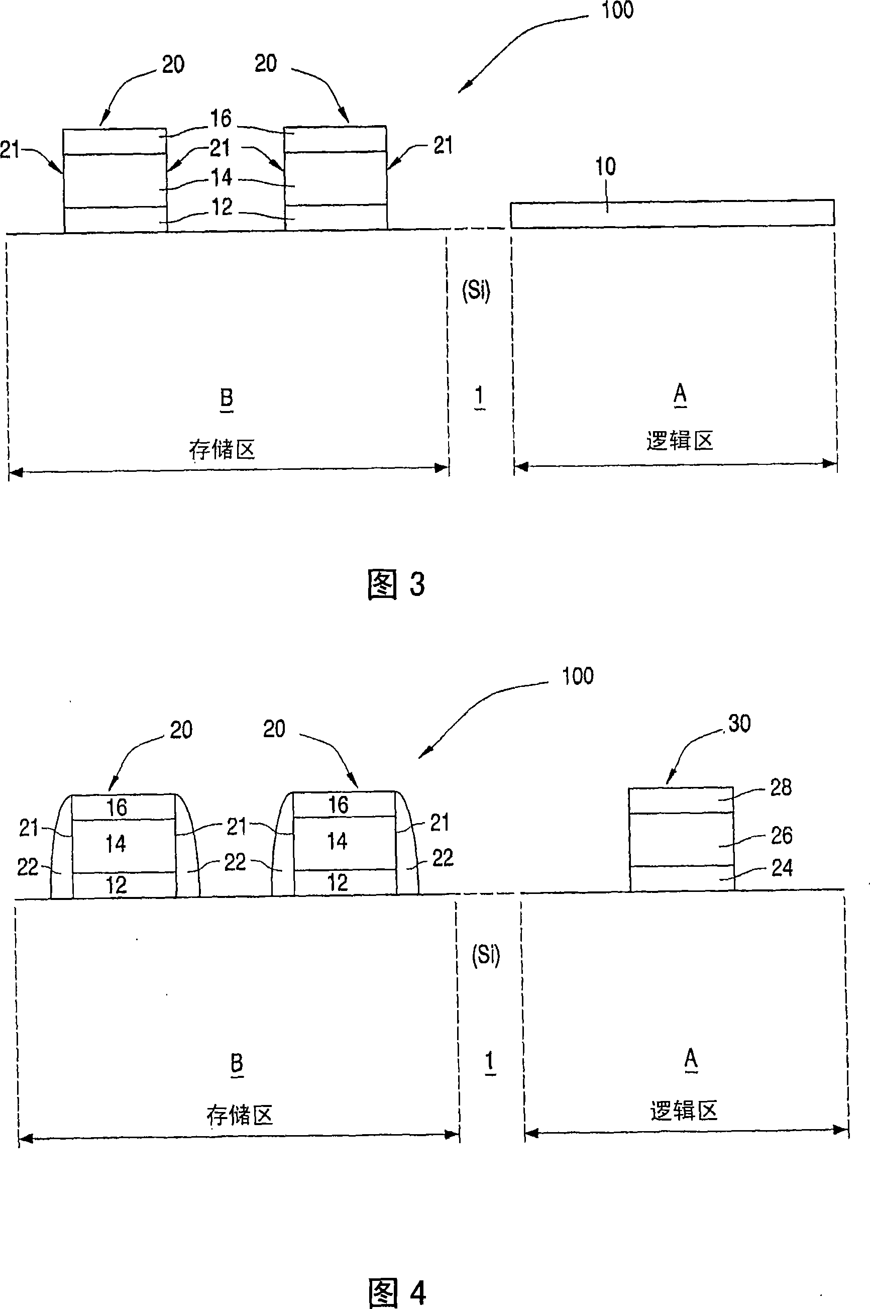
[0039] Figure 3 diagrammatically shows a cross-sectional view of a microelectronic device comprising a SONOS memory cell according to the invention at a first moment during manufacture.

[0040] A microelectronic device 100 comprising a logic area A and a memory area B is produced on a semiconductor substrate 1 .

[0041] The logic area A includes device components constituting a logic circuit, and the memory area B includes device components such as the SONOS memory cell 20...


PUM


Abstract

Method of manufacturing a non-volatile memory device on a semiconductor substrate in a memory area, said non-volatile memory device comprising a cell stack of a first semiconductor layer, a charge trapping layer and an electrically conductive layer, the charge trapping layer being the intermediate layer between the first semiconductor layer and the electrically conductive layer, the charge trapping layer comprising at least a first insulating layer; the method comprising: providing the substrate having the first semiconductor layer; depositing the charge trapping layer; depositing the electrically conductive layer; patterning the cell stack to form at least two non-volatile memory cells, and creating a shallow trench isolation in between said at least two non-volatile memory cells.

Description

technical field [0001] The invention relates to a method of manufacturing a non-volatile memory device as defined in the preamble of claim 1 . In addition, the present invention relates to such a non-volatile memory device. Furthermore, the invention relates to an integrated circuit comprising at least one such non-volatile memory device. Background technique [0002] The SONOS memory device includes a non-volatile memory composed of stacked semiconductor oxide (silicon oxide) nitride (silicon nitride) oxide (silicon oxide) semiconductor (Semiconductor (silicon) Oxide (silicon) Nitride (silicon) Oxide Semiconductor) The memory cell, wherein the stacked ONO portion sequentially includes: a first silicon dioxide layer having a thickness of about 2 nm, a silicon nitride layer of about 6 nm, and a second silicon dioxide layer of about 8 nm. A first silicon dioxide layer is located on the semiconductor (substrate) layer. There is also a semiconductor layer (eg, polysilicon) ov...

Claims


Application Information

Patent Timeline
Patent Type & Authority Applications(China)
IPC IPC(8): H01L27/115H01L21/8246H01L27/105H01L21/8247
CPCH01L27/11573H01L27/105H01L27/11568Y10S438/954H10B43/40H10B43/30H01L29/66833
Inventor 皮埃尔·戈阿兰罗伯茨·T·F·范沙吉克
Owner NXP BV
Why Eureka
Try Eureka