Substrate for inkjet printing and method of manufacturing the same

a technology of inkjet printing and substrate, which is applied in the direction of static indicating devices, photosensitive material processing, instruments, etc., can solve the problems of ink droplets of active substances that cannot be vaporized, polymeric films deposited on the second layer may have undesirable thickness increases, and the vaporization process requires long pulse duration and high cost, so as to achieve small thickness variations, large surface tension variations, and low cost

Active Publication Date: 2010-11-16
SAMSUNG DISPLAY CO LTD
View PDF25 Cites 4 Cited by
  • Summary
  • Abstract
  • Description
  • Claims
  • Application Information

AI Technical Summary

Benefits of technology

[0021]The present invention provides a substrate with large surface tension variations and small thickness variations that may be manufactured at lower costs than conventional substrates.

Problems solved by technology

A common failure occurring in the printing process is the run-out of ink droplets of the active substance toward neighboring positions on the surface of the substrate.
These vaporizing processes require long pulse duration and are costly, which offsets a cost advantage gained by using the OLED technology.
Therefore, a polymeric film deposited on the second layer may have an undesirable increase in thickness from the separators toward the peripheral zone, which may reach pixels.
Another disadvantage of EP 0989778 lies with an ink reservoir used for overflow protection.
It is time-consuming and more complicated to construct an ink reservoir because additional processes are involved.
However, the surface tension and geometry in this edge region may not be freely, selectively varied, and it has a low spatial dissolution capacity.
Surface tension variations, therefore, may not be induced using other materials, which limits applicability.
Finally, the chemical treatment considerably increases the overall manufacturing time.
However, this method may lead to limited surface tension variations, and the time-consuming exposure process may not be suitable for mass production.
However, banks at this height may negatively impact a subsequent metal deposition process.

Method used


Image

  • Substrate for inkjet printing and method of manufacturing the same
  • Substrate for inkjet printing and method of manufacturing the same
  • Substrate for inkjet printing and method of manufacturing the same

Examples


Embodiment Construction

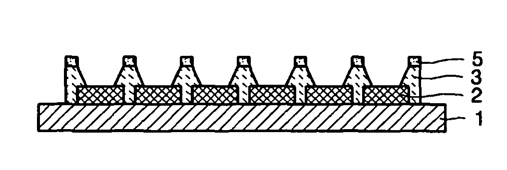
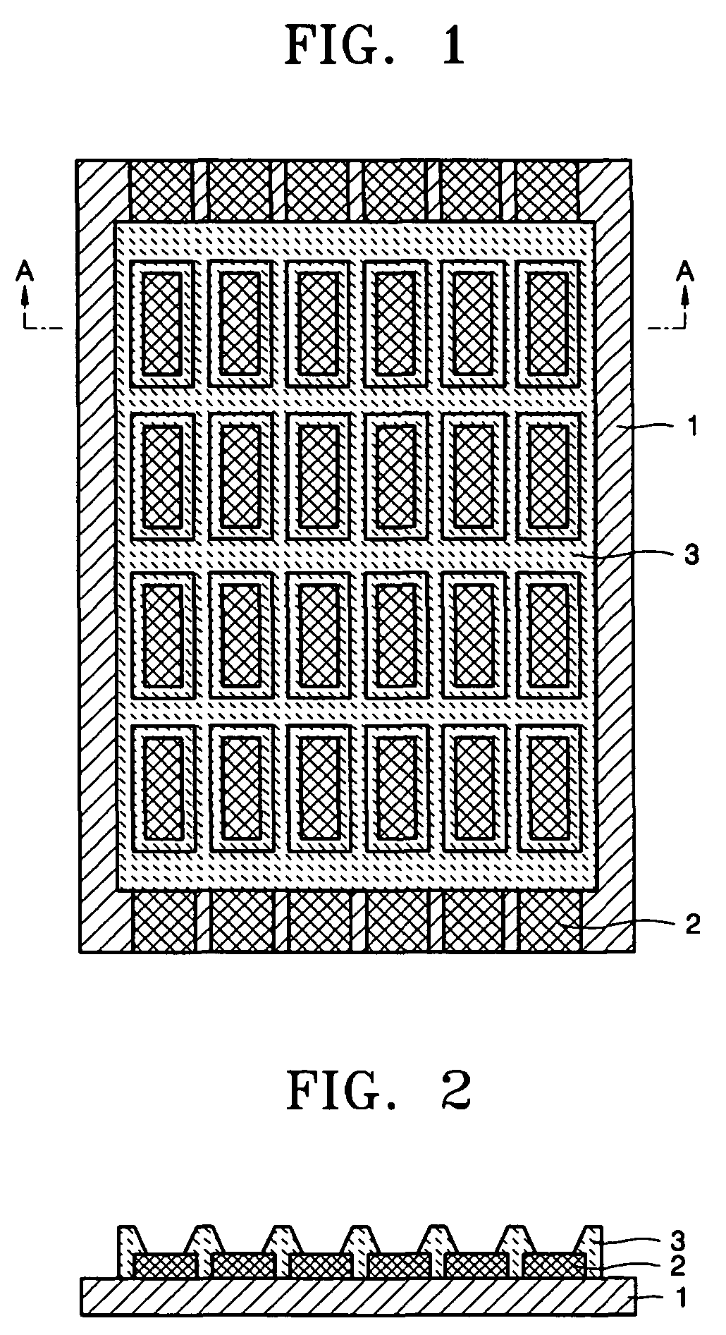
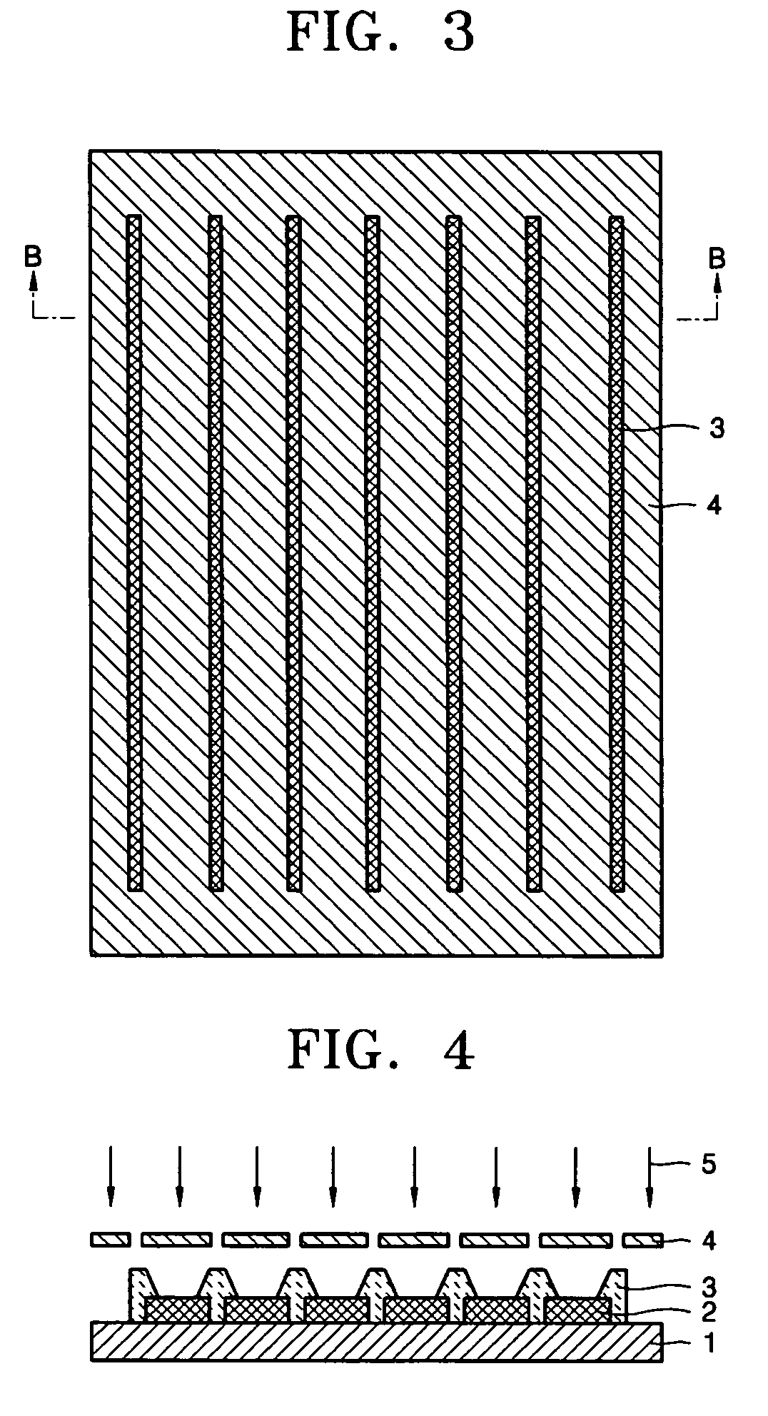
[0044]Referring to FIG. 1, which is a plan view of a 1.1-mm thick base substrate 1 formed of borosilicate glass, an intermediate layer structure 2 made of a material suitable for hole injection is on a surface of the base substrate 1. The intermediate layer structure 2 may be 100 nm thick and formed of indium-tin-oxide (ITO) or other like substances. The ITO layer structure 2 is patterned as 70 μm wide parallel stripes, spaced 10 μm apart from each other. The terms “layer structure”, “ITO layer structure”, and “photoresist layer structure” used throughout the specification refer to discontinuous layer patterns defined using a shadow mask by means of laser ablation, or other similar methods. A 0.3 μm thick photoresist layer structure 3 is formed on the base substrate 1. The photoresist layer structure 3 may be made of a photosensitive organic material, such as photoresist JSR PC 302®, using a standard technique such as lacquer coating, and it may be formed using standard techniques s...


PUM

PropertyMeasurementUnit
surface tensionaaaaaaaaaa

Abstract

A substrate for inkjet printing, which includes a photoresist layer structure on a base substrate, and a method of manufacturing the same are provided. The substrate, which has high surface tension variation and slight thickness variation, may be manufactured at a low cost. The substrate includes a discontinuous organic layer structure made of a fluorinated hydrocarbon or a polysiloxane on the photoresist layer structure.

Description

[0001]This application claims the benefit of German Patent Application No. 103 43 351.1, filed on Sep. 12, 2003, and Korean Patent Application No. 2004-521, filed on Jan. 6, 2004, which are hereby incorporated by reference for all purposes as if fully set forth herein.BACKGROUND OF THE INVENTION[0002]1. Field of the Invention[0003]The present invention relates to a substrate for inkjet printing and a method of manufacturing the same.[0004]2. Discussion of the Related Art[0005]Inkjet printing is one of most significant structuring processes used to produce full-color displays that use light-emitting, semi-conducting polymers (LEPs). The process entails depositing small drops of a solution of the corresponding polymer onto a suitable substrate. The inkjet printing process, however, may also be used to deposit a color filter or a DNA sensor onto a substrate.[0006]These applications require exact placement of a target substance, such as ink, on an activated surface of the substrate. The...

Claims


Application Information

Patent Timeline
Patent Type & Authority Patents(United States)
IPC IPC(8): B32B7/14B32B7/02G09G3/30G03F7/40B41M3/00B41M5/52H01L21/027H01L51/00H01L51/40H01L51/50H05B33/02H05B33/10H05B33/12H05B33/22
CPCB41M5/506B41M5/52H01L51/0005Y10T428/24851Y10S428/917Y10T428/24942H10K71/135
Inventor UHLIG, ALBRECHTREDECKER, MICHAELSCHAEDIG, MARCUSSCHRADER, THOMASHUMBS, WERNER
Owner SAMSUNG DISPLAY CO LTD
Why Eureka
Try Eureka