

Anti-infrared light filter for packing image sensor
An image sensing and infrared technology, applied in the direction of optical filters, image communication, color TV components, etc., can solve the problems of thick overall package structure, unbearable coating, high hardness, etc., to improve coating peeling and avoid dispersion Phenomena, Effects of Refractive Index Stabilization
- Summary
- Abstract
- Description
- Claims
- Application Information
AI Technical Summary
Problems solved by technology
Method used
Image

Examples
Embodiment 1
[0025] The production process of this example is to mix all the ingredients in the following table 1 completely, put it in a crucible with a capacity of about 100ml, melt the mixture at a temperature of 1480°C for 3 hours, and then cool it down to 1150°C in 2 hours. Then the molten crystal liquid is taken out and injected into the preheated mold body with a temperature of 550°C. Next, place it in an annealing furnace at 480°C for 16-18 hours, and then cool down naturally for 4-5 hours to room temperature. Furthermore, the above-mentioned raw rough crystal embryos are flattened for subsequent processing operations, and then the crystal embryos are subjected to procedures such as processing and grinding, precision polishing, and light-transmitting molding and cleaning to form lenses. Subsequently, a protective film of titanium oxide, silicon oxide, and niobium oxide is deposited by general evaporation or sputtering (in this case, evaporation) as an anti-environment protection la...
Embodiment 2
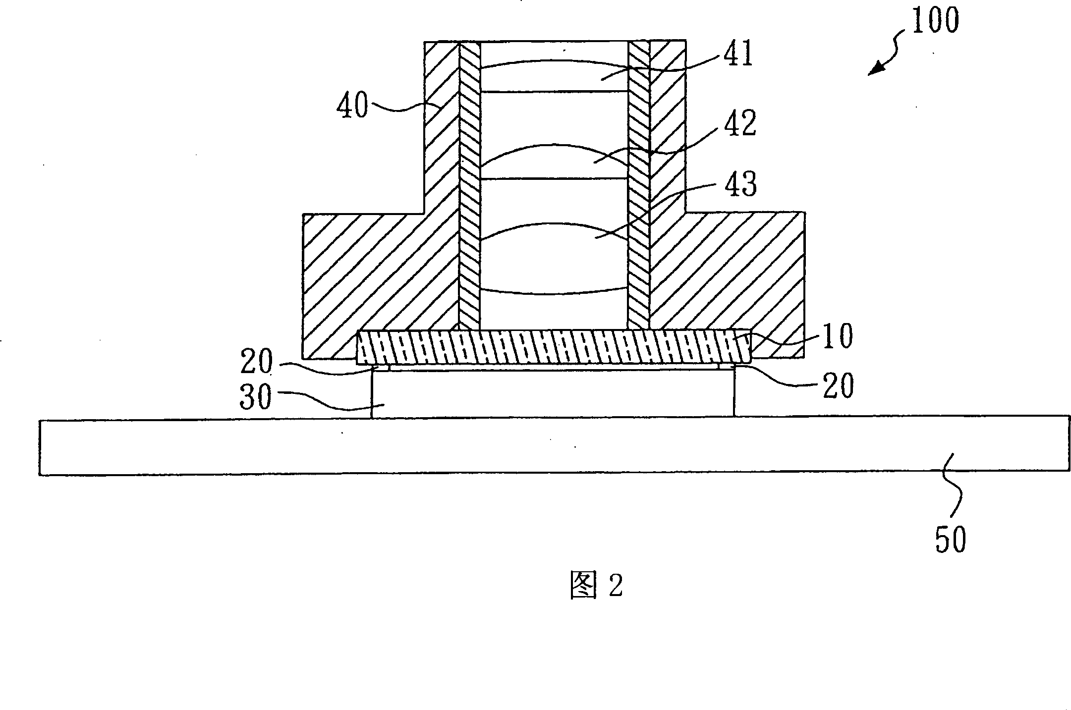
[0028] Please refer to FIG. 2. FIG. 2 is a schematic diagram of an image sensing module 100 in a preferred embodiment of the present invention, wherein an image sensing module 100 with a base 50 also includes an optical lens 40 and an anti-infrared filter chip 10. A packaging material 20, and an image sensing component 30, and the optical lens 40 contains several optical lenses 41, 42, 43. In addition, the anti-infrared filter chip 10 used in this example is the 0.30 mm thick anti-infrared filter chip 10 prepared in Embodiment 1, and the image sensing device is a charge-coupled device (CCD).
[0029] As shown in FIG. 2 , in the image sensing module 100 of the present invention, the anti-infrared filter chip 10 is interposed between the optical lens 40 and the image sensing component 30 . In addition, one side of the anti-infrared filter chip 10 is coated with a layer of packaging material 20 (in this example, epoxy resin is used), and after a packaging process, the anti-infrar...
Embodiment 3
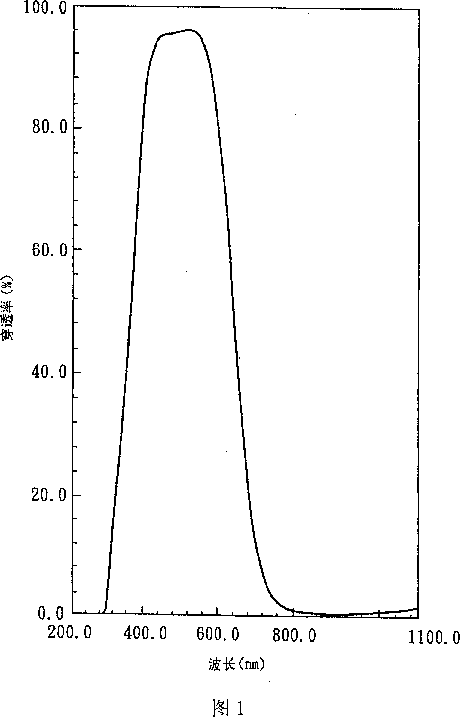
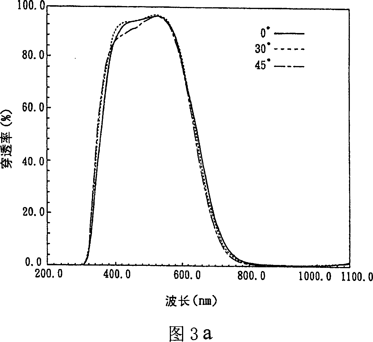
[0032] Please refer to FIG. 3 . FIG. 3 is a spectral comparison result of the anti-infrared filter chip according to the first embodiment of the present invention and the reflective infrared filter lens in a conventional coating process. Fig. 3a is a transmission spectrum diagram of incident light at different angles (0°, 30°, 45°) for the anti-infrared filter chip of the present invention. Fig. 3b is a transmission spectrum diagram of the incident light at different angles (0°, 30°) for the reflective infrared filter lens in the traditional coating process. As shown in FIG. 3 a , the spectrum difference between the forward and oblique shades of the anti-infrared filter chip of the present invention is very small, wherein the transmission spectra of the 0° forward light and the 30° oblique shades almost overlap. As shown in Figure 3b, the reflective infrared filter lens in the traditional coating process has a significant difference in the wavelength width of the transmission ...
PUM
 Abstract
Description
Claims
Application Information