
Reflow method, pattern generating method, and fabrication method for TFT element for LCD

A technology for patterning and resist film, which is applied in the field of manufacturing TFT elements for liquid crystal display devices, can solve the problems of increased manufacturing cost, complicated manufacturing process of semiconductor devices, etc., achieves fast flow, omits and reduces the number of processes, and shortens processing time. Effect

Inactive Publication Date: 2007-10-03
TOKYO ELECTRON LTD
View PDF1 Cites 5 Cited by
  • Summary
  • Abstract
  • Description
  • Claims
  • Application Information

AI Technical Summary

Problems solved by technology

However, with the development of high integration and miniaturization, the manufacturing process of semiconductor devices tends to be complicated, and the manufacturing cost increases

Method used


Image

  • Reflow method, pattern generating method, and fabrication method for TFT element for LCD
  • Reflow method, pattern generating method, and fabrication method for TFT element for LCD
  • Reflow method, pattern generating method, and fabrication method for TFT element for LCD

Examples


Embodiment Construction

[0090] Next, preferred embodiments of the present invention will be described with reference to the drawings.

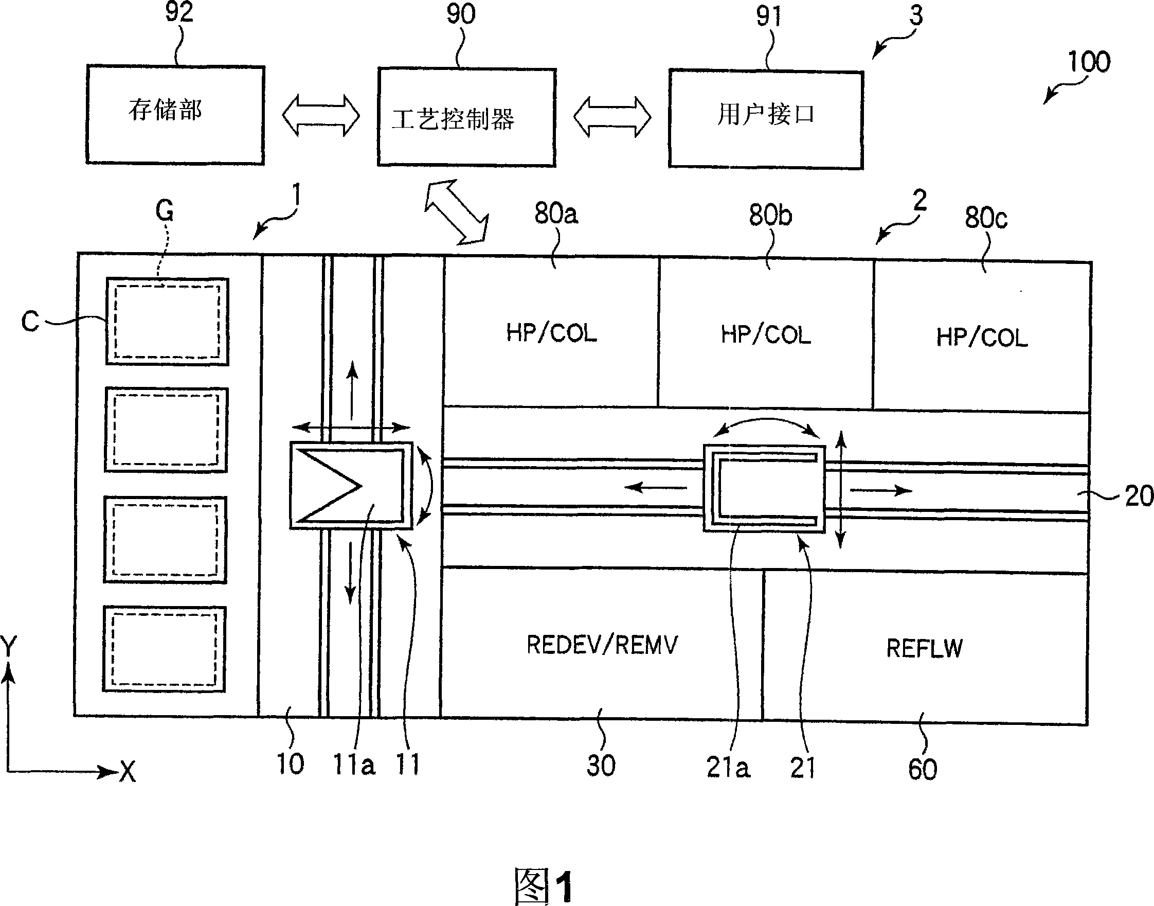
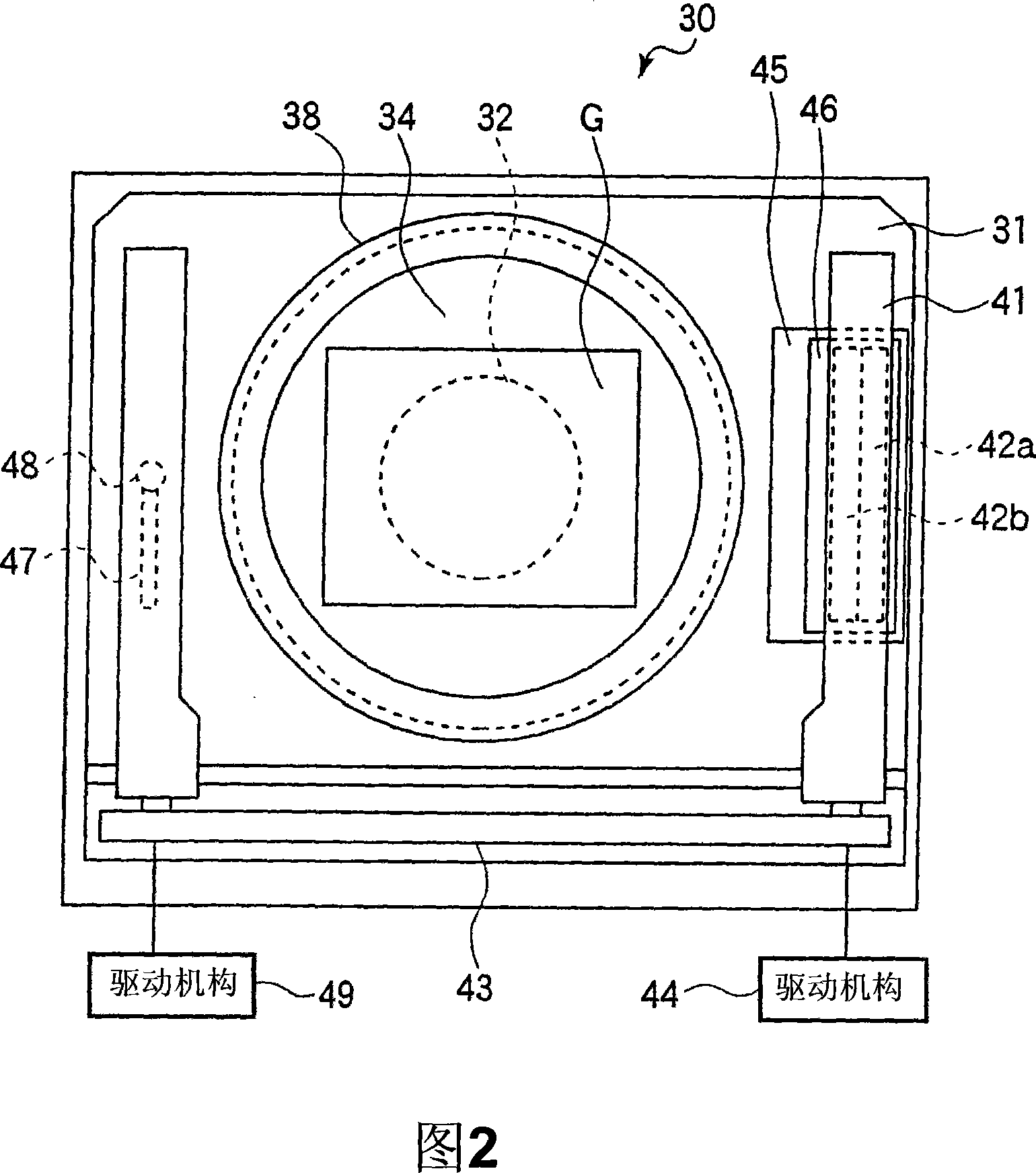
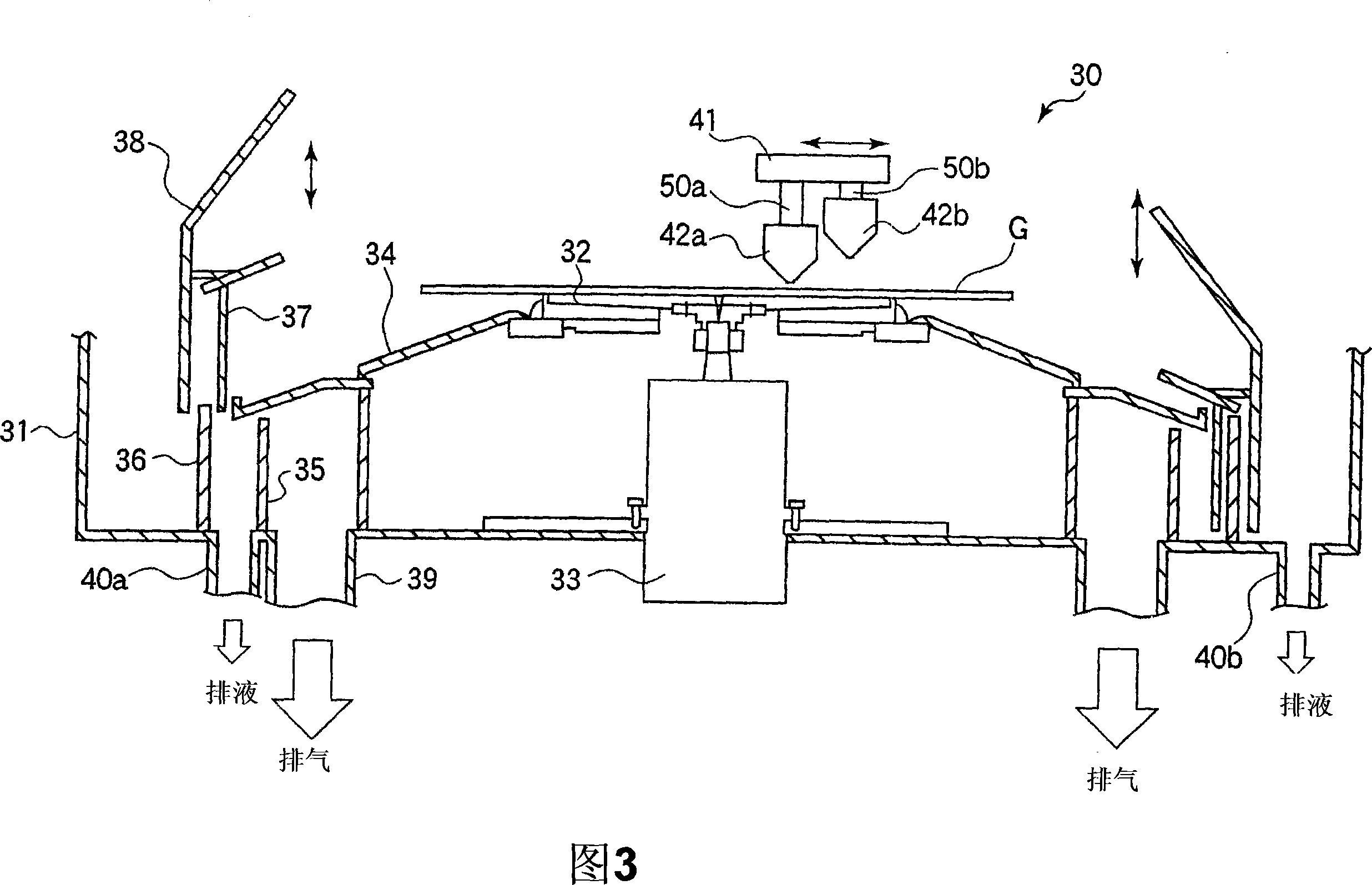
[0091] Fig. 1 is an overall schematic plan view of a releveling treatment system suitable for the releveling method of the present invention. In this embodiment, the resist film formed on the surface of the glass substrate for LCD (hereinafter abbreviated as "substrate") G is softened and deformed after the development treatment, and re-leveling treatment is carried out for re-covering. The re-leveling treatment unit and the re-leveling treatment system of the re-development treatment / release agent unit (REDEV / REMV) for performing the re-development treatment and pre-treatment performed before the re-leveling treatment will be described as an example. This reflow processing system 100 includes a cassette loading and unloading station (loading and unloading section) 1 on which a cassette C accommodating a plurality of substrates G is mounted, and is used to perform re...


PUM


Abstract

To provide a technology that can precisely control the flow direction and area of a softened resist, and thereby can be utilized for forming a pattern and manufacturing a TFT element for liquid crystal displays in the reflow treatment of the resist. A resist 103 subjected to reflow treatment is formed in an overhang shape while a lower edge J at a side facing a target region S1overhangs to the side of the target region S1as compared with the edge of a lower-layer film 102. By allowing the lower edge J of the resist 103 to project from the lower-layer film 102, the resist 103 does not stagnate, thus allowing a softened resist to flow toward the target region S1rapidly. The flow of the resist 103 toward the prohibited area S2is suppressed as a reaction for accelerating the flow of the resist 103 toward the target region S1, thus stopping deformation without reaching the prohibited area S2.

Description

technical field [0001] The present invention relates to a resist reflow method that can be used in the formation of a pattern for semiconductor devices such as thin film transistor (TFT) elements, a method for forming a pattern using the reflow method, and a liquid crystal display device A method of manufacturing a TFT element. Background technique [0002] In recent years, semiconductor devices are developing toward higher integration and miniaturization. However, with the development of high integration and miniaturization, the manufacturing process of semiconductor devices tends to be complicated, and the manufacturing cost increases. Therefore, people have been researching technical solutions that can significantly reduce manufacturing costs, integrate mask patterning steps for photolithography, and shorten the overall number of steps. [0003] As a technique for reducing the number of steps for forming a mask pattern, it has been proposed to soften the resist by infil...

Claims


Application Information

Patent Timeline
Patent Type & Authority Applications(China)
IPC IPC(8): H01L21/027H01L21/336H01L21/308H01L21/3213G02F1/1362
CPCH01L21/0273H01L29/41733H01L29/66765
Inventor 麻生丰
Owner TOKYO ELECTRON LTD
Learn More