Semiconductor package stack with through-via connection
A through-hole, semiconductor technology, applied in the direction of semiconductor devices, semiconductor/solid-state device components, electric solid-state devices, etc., can solve the problems that it is not easy to reduce the overall size and packaging area, require space, limit miniaturization, etc.
- Summary
- Abstract
- Description
- Claims
- Application Information
AI Technical Summary
Problems solved by technology
Method used
Image
Examples
Embodiment Construction
[0026] Next, preferred embodiments of the present invention will be described with reference to the relevant drawings. In the following descriptions and drawings, the same reference numerals will be used to designate the same or similar components, and repeated descriptions of the same or similar components will be omitted.
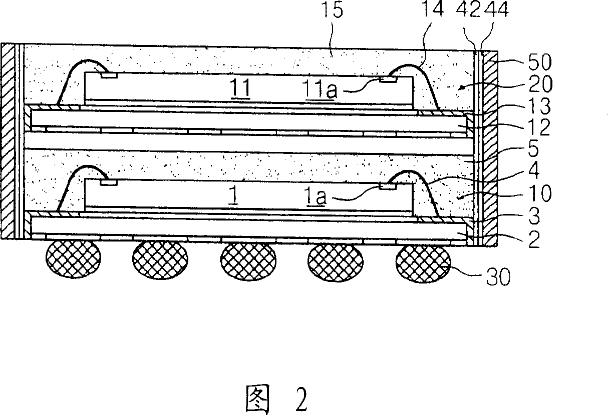
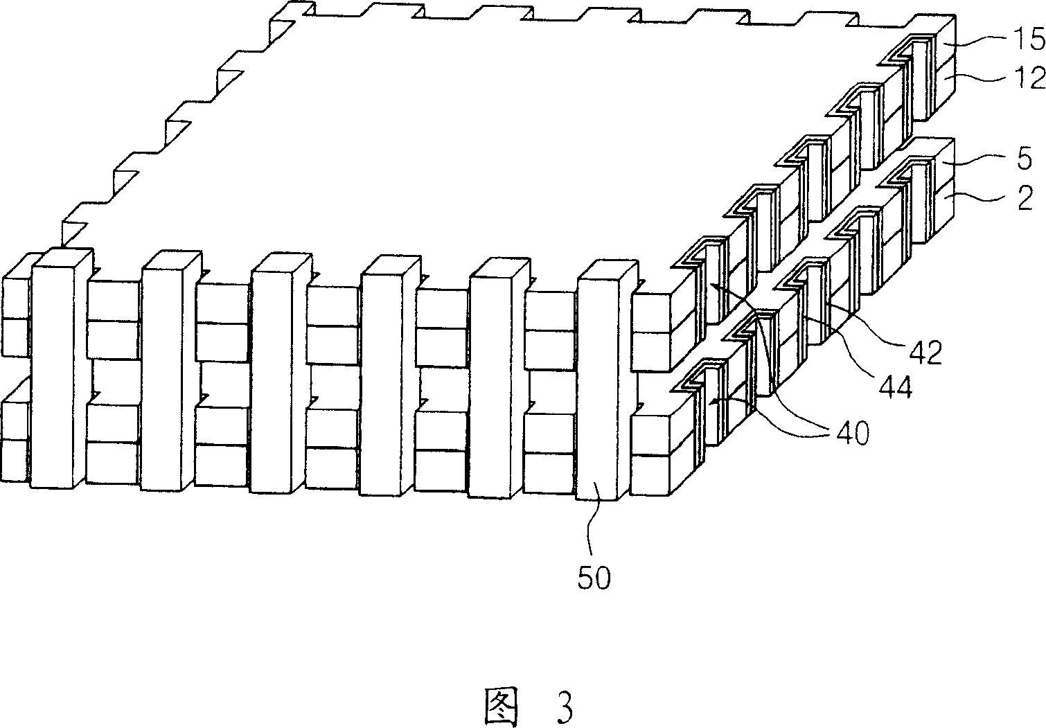
[0027] According to an embodiment of the present invention, when FBGA packages are stacked together, plated through holes are formed on the side of each package, and conductive leads are disposed in each plated through hole for electrical connection between the package stacks.
[0028] Because the present invention does not need to add extra space when performing package stacking. Therefore, the overall size and thickness of the package stack can be reduced to meet the volume requirement of the current semiconductor technology. In addition, compared with the conventional technology, the present invention does not use either the substrate or the connectio...
PUM
 Abstract
Description
Claims
Application Information


