Nonvolatile semiconductor storage device and method for manufacturing the same

A non-volatile, storage device technology, applied in semiconductor/solid-state device manufacturing, semiconductor devices, static memory, etc., can solve problems such as inability to suppress parasitic transistors, failure to form, etc., and achieve the effect of favorable charge retention characteristics

Inactive Publication Date: 2007-10-03
SEMICON ENERGY LAB CO LTD
View PDF2 Cites 19 Cited by
  • Summary
  • Abstract
  • Description
  • Claims
  • Application Information

AI Technical Summary

Problems solved by technology

In the case of using an SOI substrate, if the thickness of the semiconductor layer is made large, there is a problem: the parasitic transistor between the source region and the drain region cannot be suppressed, so a completely depleted layer type TFT cannot be formed

Method used


Image

  • Nonvolatile semiconductor storage device and method for manufacturing the same
  • Nonvolatile semiconductor storage device and method for manufacturing the same
  • Nonvolatile semiconductor storage device and method for manufacturing the same

Examples


Embodiment approach 1

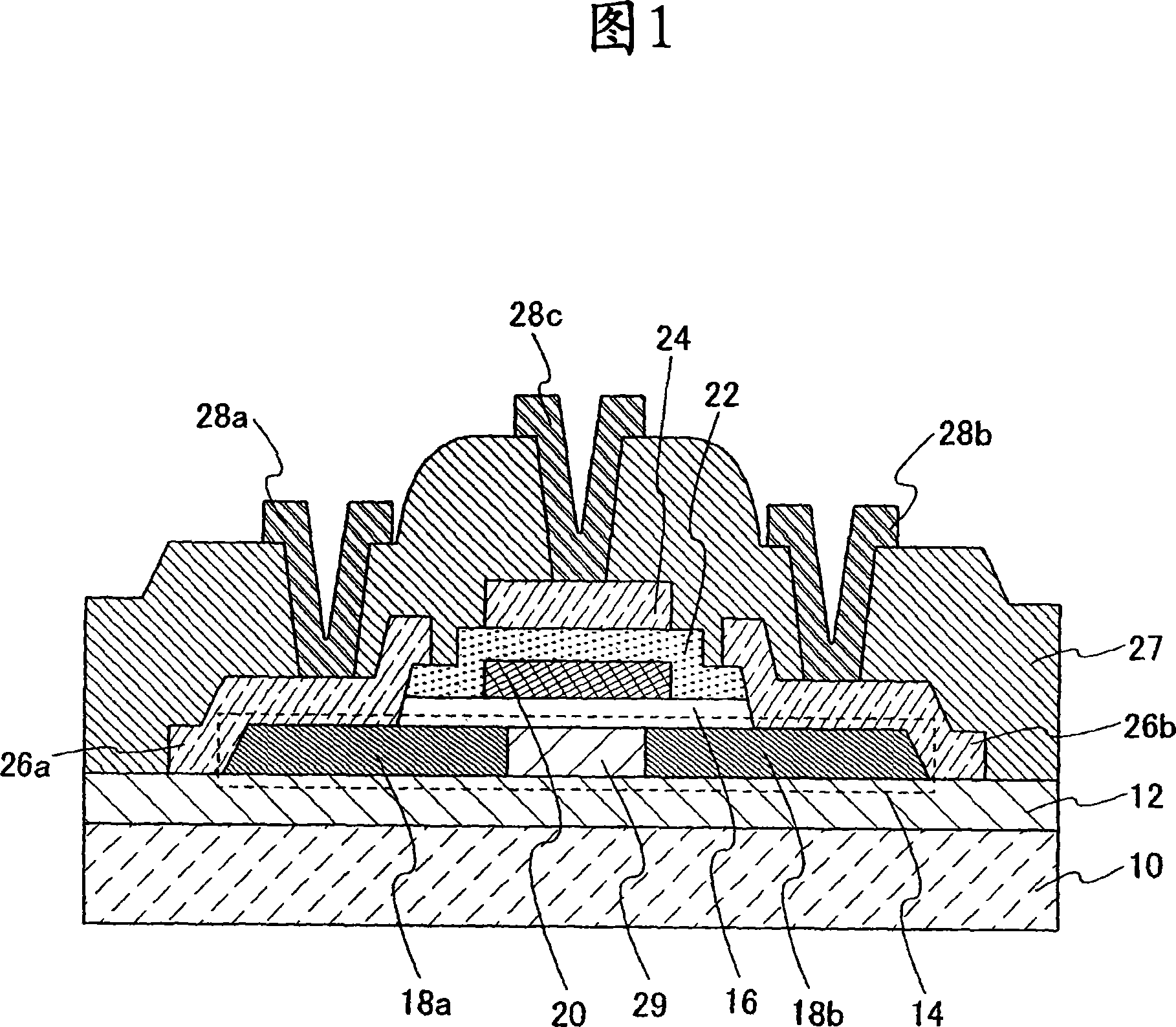
[0051] FIG. 1 is a sectional view illustrating the main structure of a nonvolatile semiconductor memory device related to the present invention. FIG. 1 illustrates, inter alia, the main part of the nonvolatile memory element.

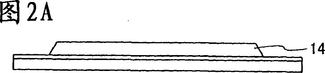
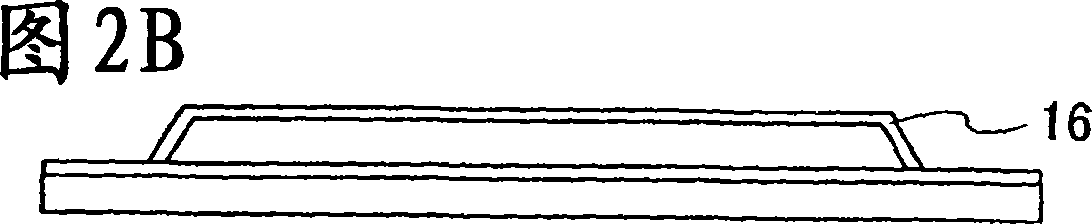
[0052] In FIG. 1, reference numeral 10 denotes a substrate, 12 is a base insulating film, 14 is a semiconductor layer, 29 is a channel formation region, 18a and 18b are source regions or drain regions, and 16 is a first insulating film (also called tunnel insulating film), 20 is a floating gate electrode, 22 is a second insulating film (also known as a control insulating film), 24 is a control gate electrode, 26a and 26b are conductive layers, 28a and 28b are through conductive layers 26a and 26b A source or drain electrode electrically connected to the source or drain regions 18a and 18b, 28c is a gate wiring electrically connected to a control gate electrode, and 27 is an insulating film for passivation.

[0053] In the structure shown in FIG. 1 , ba...

Embodiment approach 2

[0106] In this embodiment mode, a method of manufacturing a nonvolatile memory element having a structure different from that of the nonvolatile memory element shown in FIG. 1 will be described. In this embodiment mode, a nonvolatile memory element as shown in FIG. 11 will be explained. In the nonvolatile memory element shown in FIG. 11 , the control gate electrode 24 has side walls 300 .

[0107] 11, reference numeral 10 denotes a substrate; 12, a base insulating film; 14, a semiconductor layer; 29, a channel formation region; 18a and 18b, a source region or a drain region; 20 is a floating gate electrode; 22 is a second insulating film (also called a control insulating film); 24 is a control gate electrode; 300 is a side wall; 26a and 26b are conductive layers; 28a and 28b are through Conductive layers 26a and 26b are connected to source or drain electrodes of source or drain regions 18a and 18b; 28c is a gate wiring electrically connected to a control gate electrode; 27 is...

Embodiment approach 3

[0122] In this embodiment mode, a structure of a nonvolatile memory different from the structure shown in FIGS. 1 and 11 will be described with reference to FIGS. 14A and 14B, FIGS. 15A to 15D, and FIGS. 16A and 16B.

[0123] In the nonvolatile memory element shown in FIG. 14A, first impurity regions (source or drain regions) 306a and 306b, second impurity regions 307a and 307b, etc. are provided in the semiconductor layer 14, and the floating gate electrode 20 is composed of A floating gate electrode 20a and a second floating gate electrode 20b are formed, which are different from the structures shown in FIGS. 1 and 11 .

[0124] In the structure shown in FIG. 14A, a base insulating film 12 is formed on a substrate 10, and a base insulating film 12 having first impurity regions 306a and 306b, second impurity regions 307a and 307b, and a channel formation region 29 is formed on the base insulating film 12. The semiconductor layer 14. The first insulating film 16 and the condu...


PUM


Abstract

It is an object to provide a nonvolatile semiconductor storage device that prevents increase in a contact resistance value due to etching of a semiconductor layer when etching an interlayer insulating film and that has superiority in a writing characteristic and an electric charge-holding characteristic, and a manufacturing method thereof. A conductive layer is provided between a source or drain region and a source or drain wiring. The conductive layer is made of the same conductive layer that forms a control gate electrode. An insulating film is provided so as to cover the conductive layer, and the insulating film has a contact hole for exposing part of the conductive layer. The source or drain wiring is formed so that the contact hole is filled.

Description

technical field [0001] The present invention relates to a nonvolatile semiconductor memory device capable of electrical writing, reading and erasing, and a manufacturing method thereof. Background technique [0002] The market for non-volatile memory is expanding. In a nonvolatile memory, data can be rewritten electrically, and data can be retained even after power is turned off. There is a feature that a nonvolatile memory has a structure similar to a MOSFET (Metal Oxide Semiconductor Field Effect Transistor), providing a region capable of accumulating charge for a long period of time on a channel formation region. The charge accumulation region of a nonvolatile memory is also called a floating gate because it is formed on an insulating layer and is insulated from the surroundings. A control gate is provided on the floating gate via an insulating layer (for example, Patent Document 1 and Patent Document 2: Japanese Patent Application Laid-Open Nos. H5-189984 and No. H6-61...

Claims


Application Information

Patent Timeline
Patent Type & Authority Applications(China)
IPC IPC(8): H01L27/115H01L27/12H01L29/788H01L29/40H01L21/8247H01L21/84H01L21/336H01L21/28
CPCH01L27/115H01L2924/0002H01L29/7881H01L21/84G11C16/0483H01L27/12H10B69/00H01L2924/00H10B41/30
Inventor 浅见良信
Owner SEMICON ENERGY LAB CO LTD
Why Eureka
Try Eureka