Method of making light emitting device with silicon-containing encapsulant

A manufacturing method and a technology of a light-emitting device, which can be applied to circuits, electric solid-state devices, semiconductor devices, etc., and can solve problems such as lead wire breakage

Inactive Publication Date: 2007-10-24
3M INNOVATIVE PROPERTIES CO
View PDF25 Cites 13 Cited by
  • Summary
  • Abstract
  • Description
  • Claims
  • Application Information

AI Technical Summary

Problems solved by technology

[0003] A second problem that can occur when using conventional epoxies is stress-induced fracture of the wire bond during repeated thermal cycling

Method used


Image

  • Method of making light emitting device with silicon-containing encapsulant

Examples


Embodiment 1

[0059] Example 1: Visible light curing

[0060] Prepare in a 35 mL brown bottle from 10.00 g (milli-equivalent weight of olefin = 3.801 g) of organopolysiloxane prepared as described in the previous paragraph and 0.44 g (milli-equivalent weight of Si-H = 0.111 g) (CH 3 ) 3 SiO-[Si(CH 3 ) 2 O] 15 -[SiH(CH 3 )O] 25 -Si(CH 3 ) 3 (SYL-OFF(R) 7678 from Dow Corning Company). By adding 22.1mg Pt(acac) 2 (wherein acac is acetylacetonate, purchased from Aldrich Chemical Company) dissolved in 1.00mL CH 2 Cl 2Catalyst stock solutions were prepared in . A 100 [mu]L aliquot of this catalyst stock was added to the silicone mixture. The final formulation corresponds to a ratio of aliphatic unsaturation to silicon-bonded hydrogen of 1.5 and contains about 100 ppm platinum.

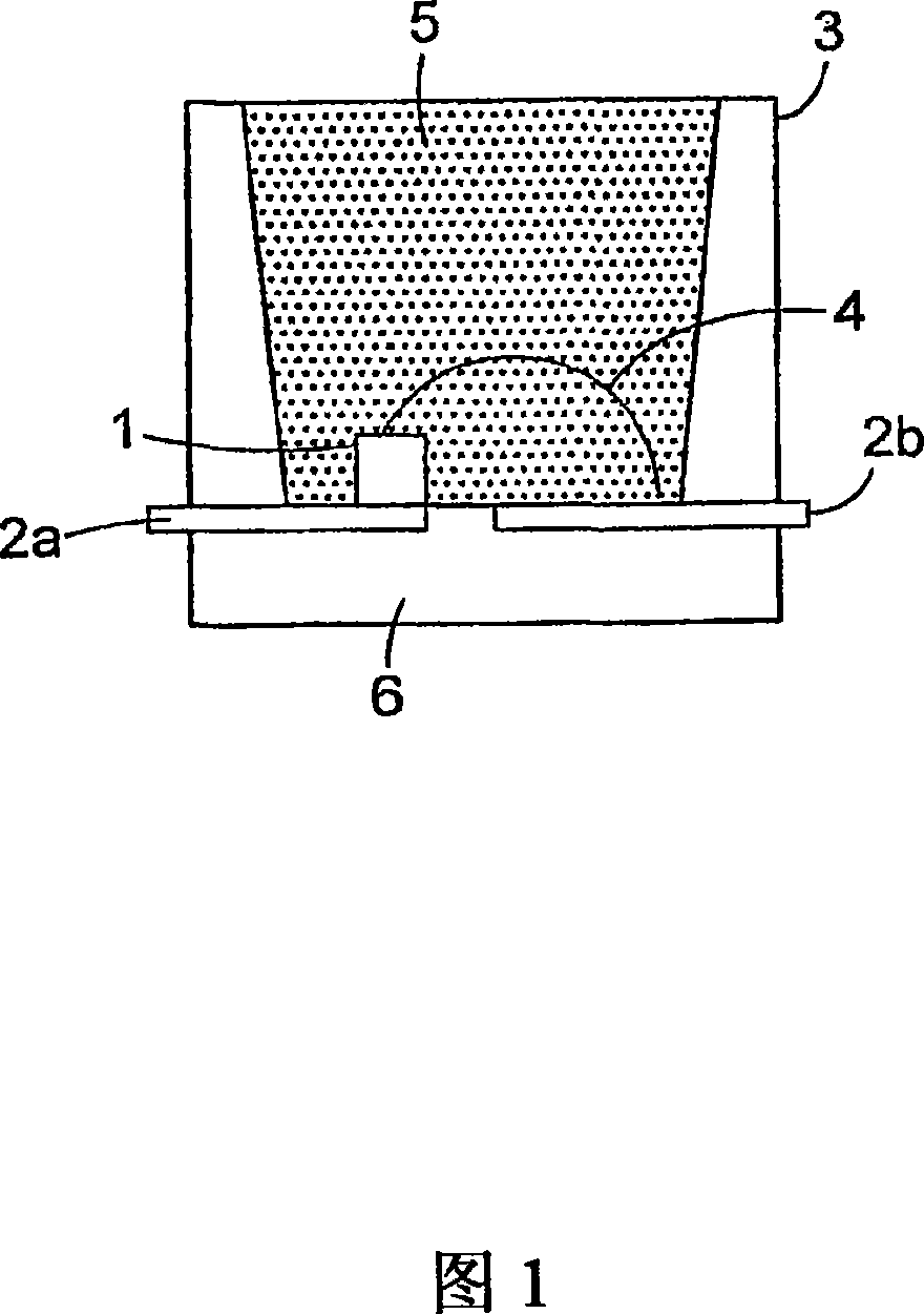
[0061] About 2 mg of the above final formulation was placed in the LED assembly. The LED was illuminated at 20 mA for 2.5 minutes. The sealed device was left to stand for an additional 5 minutes. The seala...

Embodiment 2

[0062] Embodiment 2: UV light curing

[0063] A sealed LED device was fabricated and evaluated in the same manner as described in Example 1, except that 21.1 mg of CpPt(CH 3 ) 3 , without using 22.1mg Pt(acac) 2 , and the difference is that the UV lamp is used to irradiate at 365nm, wherein the CpPt(CH 3 ) 3 was prepared according to the method described by Boardman et al. (Magn. Reson. Chem., 30, 481 (1992)). The efficiency of the device was measured to increase from 8.9% before sealing to 11.6% after sealing.

Embodiment 3

[0066] Example 3: Visible light curing

[0067] Prepared from 10.00 g (milliequivalent weight of olefin = 1.46 g) of vinylsiloxane base polymer H in a 35 mL brown bottle 2 C=CH-Si(CH 3 ) 2 O-[Si(CH 3 )(C 6 h 5 )O] n -Si(CH 3 ) 2 -CH=CH 2 (PMV-9925, produced by Gelest Company) and 1.64g (mequivalent weight of Si-H = 0.16g) silicone crosslinking agent (CH 3 ) 2 SiO-[SiH(CH 3 )O] m -[Si(CH 3 )(C 6 h 5 )O] n -Si(CH 3 ) 2 A silicone mixture consisting of H (HPM-502, produced by Gelest Company). Prepare Pt(acac) according to the method described in Example 1 2 in CH 2 Cl 2 , and a 100 μL aliquot of the resulting solution was added to the siloxane mixture. The final formulation corresponds to a ratio of aliphatic unsaturation to silicon-bonded hydrogen of 1.5 and contains about 100 ppm platinum.

[0068] About 2 mg of the above final formulation was placed in the LED assembly. The LED was illuminated at 20 mA for 2.5 minutes and then left to stand for an addit...


PUM

PropertyMeasurementUnit
wavelengthaaaaaaaaaa

Abstract

A circuit architecture ( 200 ) for implementation of compensation based on Miller capacitors in multi-stage chopped amplifiers includes insertion of an additional chopper ( 206 ) in the compensation feedback ( 118, 120 ) pathway. Such compensation is more area efficient than parallel compensation and allows higher bandwidth in multistage amplifiers. The insertion of a chopper in the Miller capacitance feedback loop provides a means to selectively adjust the phase of the feedback by 180 degrees.

Description

technical field [0001] The invention relates to a method for manufacturing a light emitting device. More specifically, the present invention relates to a method of manufacturing a light emitting device having a light emitting diode (LED) and a silicon-containing encapsulant. Background technique [0002] Conventional encapsulants used for LEDs are organic polymer materials. The lifetime of the encapsulant is a significant obstacle to improving the performance of HB LEDs. Conventional LEDs are encapsulated in epoxy and when used, tend to turn yellow over time reducing the brightness of the LED and changing the color rendering index of the light emitted by the light emitting device. This situation is especially important for white LEDs. It is believed that the yellowing of the epoxy is due to the decomposition of the epoxy due to the high operating temperature of the LED and / or absorption of the UV-blue light emitted by the LED. [0003] A second problem that can occur whe...

Claims


Application Information

Patent Timeline
Patent Type & Authority Applications(China)
IPC IPC(8): H01L33/00C08G77/04H01L23/29H01L33/52H01L33/56
CPCH01L33/52H01L33/56H01L2224/48091H01L23/293H01L2224/45144H01L2924/00014H01L2924/00
Inventor 拉里·D·博德曼D·斯科特·汤普森凯瑟琳·A·莱瑟达尔安德鲁·J·欧德科克
Owner 3M INNOVATIVE PROPERTIES CO
Why Eureka
Try Eureka