Liquid crystal display panel and picture element array structure thereof
A pixel array and array technology, applied in the field of liquid crystal display panels and their pixel array structures, can solve the problems of improving the display effect of multi-domain vertically aligned liquid crystal display panels, discontinuous liquid crystal molecules, and uncertain tilting directions of liquid crystal molecules, etc., to achieve The effect of good aperture ratio of display area, increased degree of electric field deformation, and fast response rate
- Summary
- Abstract
- Description
- Claims
- Application Information
AI Technical Summary
Problems solved by technology
Method used
Image

Examples
no. 1 example
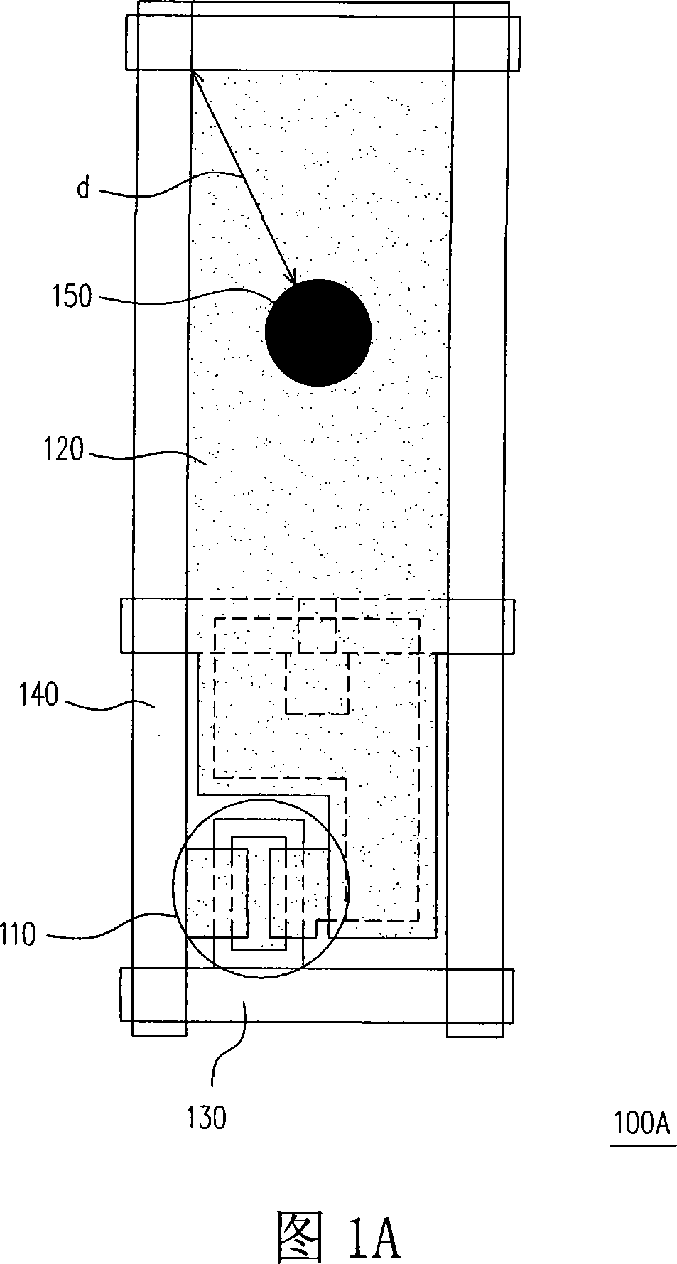
[0063] First Embodiment: FIG. 2A is a liquid crystal display panel according to a first embodiment of the present invention, and FIG. 2B is a schematic diagram of a pixel array structure of the liquid crystal display panel in FIG. 2A . Please refer to FIG. 2A , the liquid crystal display panel 200 includes a first substrate 210 , a second substrate 220 , a liquid crystal layer 230 and a pixel array structure 240A. The first substrate 210 includes a plurality of scan lines 212 and a plurality of data lines 214 , and the second substrate 220 includes a shared electrode 222 . In addition, the liquid crystal layer 230 is disposed between the first substrate 210 and the second substrate 220 .
[0064] Please refer to FIG. 2B , the pixel array structure 240A includes a plurality of pixel units 250 and a plurality of protrusions 260 . A plurality of pixel units 250 are arranged in an array and electrically connected to corresponding scan lines 212 and data lines 214 , and each pixel...
no. 2 example
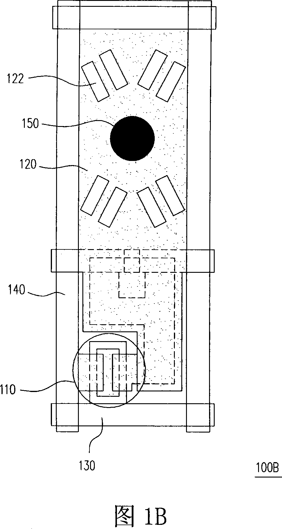
[0073] Embodiment 2: Of course, the liquid crystal display panel proposed by the present invention is not limited to having the pixel array structure described in the above embodiments. Actually, the pixel array structure applied to the liquid crystal display panel of the present invention can also have many different types. FIG. 3 is a pixel array structure of the second embodiment of the present invention. Please refer to FIG. 3 , the pixel array structure 340 of this embodiment is substantially the same as the pixel array structure 240A of the first embodiment. The difference is that in the pixel array structure 340, the protrusions 360 corresponding to the corners C of the electrode blocks 254a and 254b are a plurality of cross protruding structures.
[0074] As shown in FIG. 3 , the protrusion 360 is, for example, located between four adjacent electrode blocks 254 a and 254 b arranged in a rectangular shape, and each cross-shaped protrusion structure has a vertical porti...
no. 3 example
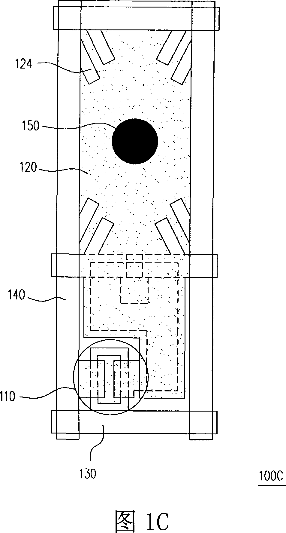
[0075] Embodiment 3: In the present invention, the pixel electrode is divided into a plurality of electrode blocks. In order to adjust the tilting direction of the liquid crystal molecules on the boundary area between the electrode block and the electrode block of the same pixel electrode, this embodiment proposes another A raised configuration.
[0076]FIG. 4A is a schematic diagram of a pixel array structure according to a third embodiment of the present invention. Please refer to FIG. 4A , the pixel array structure 440A is substantially the same as the pixel structure 240A, except that in each pixel unit 450 of the pixel array structure 440A, the protrusion 460A is, for example, located at the border area between two adjacent electrode blocks 454a and electrode blocks 454b B central. In addition, the scan line 212 corresponding to each pixel unit 450 is located between two adjacent electrode blocks 454 a and 454 b of each pixel unit 450 , for example. Wherein, the electro...
PUM
 Abstract
Description
Claims
Application Information