Method and system for processing interruption

A processing method and technology of co-processing chips, applied in electrical digital data processing, instruments, etc., can solve problems such as affecting the processing speed of embedded systems, increasing software load, and large workload, saving system power consumption and reducing software load. , the effect of improving the processing speed

Inactive Publication Date: 2007-11-21
WUXI ZGMICRO ELECTRONICS CO LTD
0 Cites 4 Cited by

AI-Extracted Technical Summary

Problems solved by technology

When the amount of data is very large, the workload of the protection site and the future recovery site will become huge, which will affect the ...

Method used

In an embodiment of the present invention, the baseband chip sends an interrupt flag to the coprocessing chip through the multiplexing bus to notify the generation of an interruption, which saves the use of pins, can further reduce the volume of the baseband chip and the c...

Abstract

A method for processing interruption includes generating interruption by base band chip and using complexing bus to send interruption start-up flag to coprocessing chip then sending interruption ended flag to said coprocessing chip by base band chip through said complexing bus when interruption treatment is finished. The system used for realizing said method is also disclosed.

Application Domain

Technology Topic

Image

  • Method and system for processing interruption
  • Method and system for processing interruption
  • Method and system for processing interruption

Examples

  • Experimental program(1)

Example Embodiment

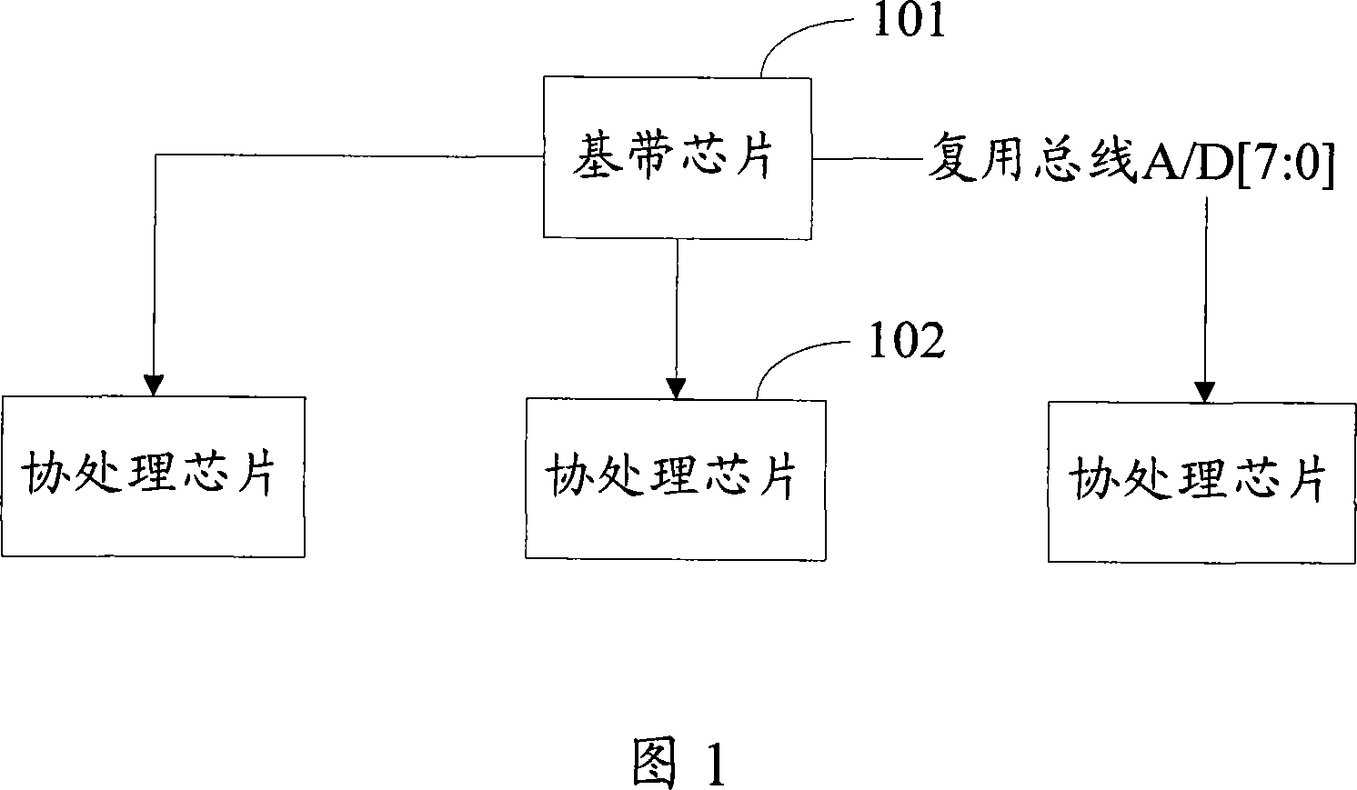
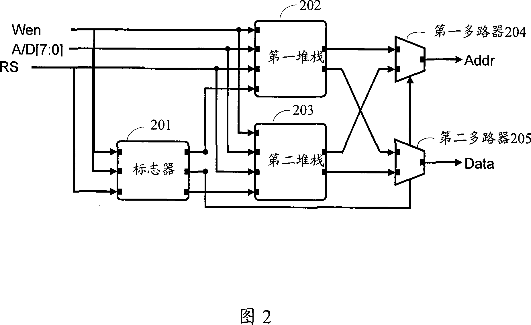
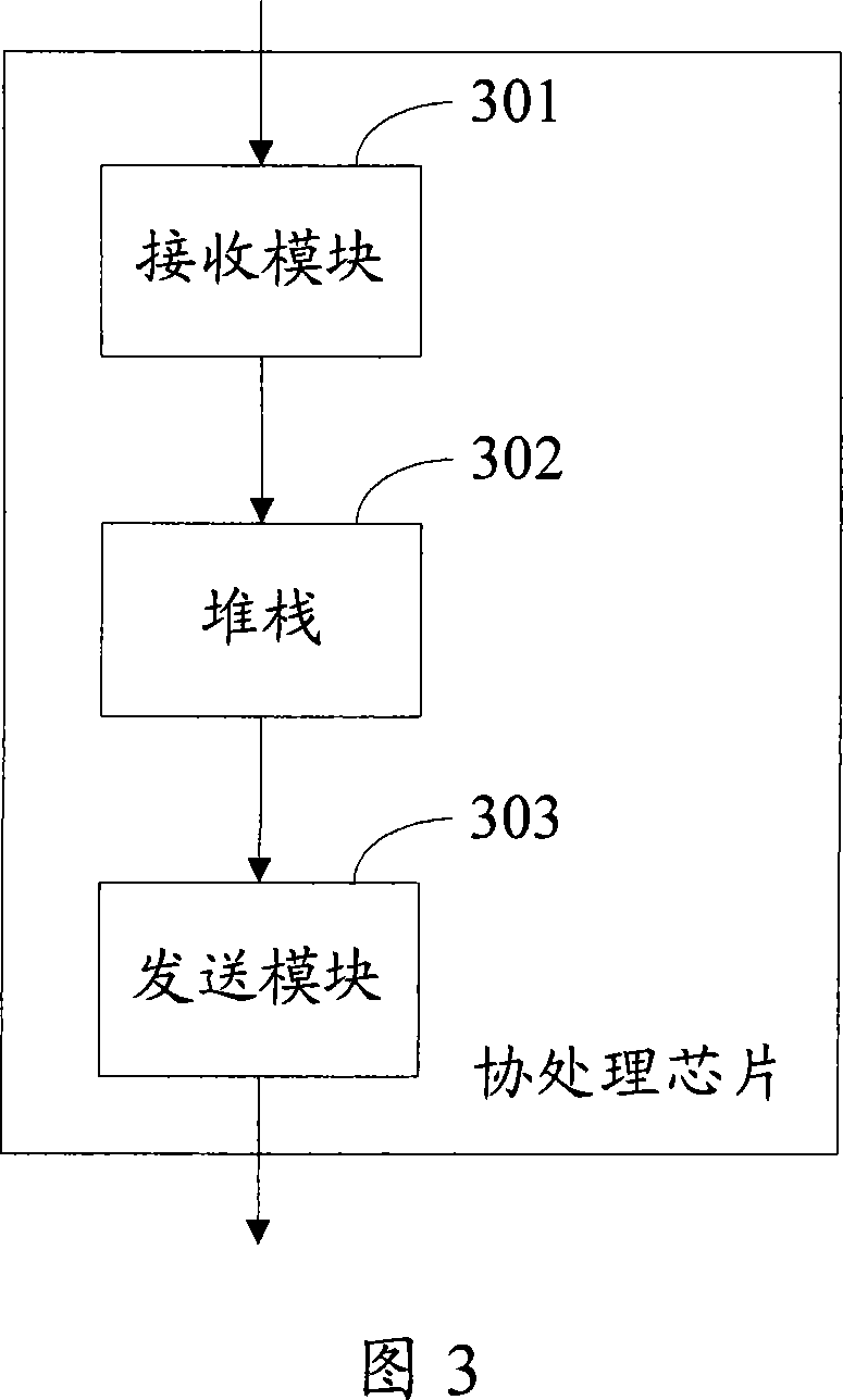
[0030] In this embodiment, when the baseband chip generates an interrupt, it sends an interrupt flag to the co-processing chip through the data/address multiplexing bus (hereinafter referred to as the multiplexing bus) to notify the co-processing chip to perform related interrupt operations. This embodiment provides a co-processing chip including at least two hardware stacks (hereinafter referred to as stacks), one stack is used to process data and addresses in normal mode, and the other stack is used to process data and addresses in interrupt mode. The normal mode in this embodiment is relative to the interrupt mode, that is, the working mode after no interrupt is generated or the interrupt ends.
[0031] The baseband chip can send an interrupt flag to the co-processing chip via the data multiplexing bus in the form of data, or can send an interrupt flag to the co-processing chip via the data multiplexing bus in the form of an address, depending on the interrupt location. In this embodiment, an interrupt flag in the form of an address is taken as an example for description.
[0032] Referring to FIG. 1, the system in this embodiment includes a baseband chip 101, a co-processing chip 102, and a multiplex bus A/D[7:0].
[0033] The multiplex bus A/D[7:0] connects the baseband chip 101 and the co-processing chip 102, and provides data and address transmission channels.
[0034] The baseband chip 101 has general processing functions and executes general programs. The co-processing chip 102 needs to be accessed during the processing in the normal mode, and the same co-processing chip 102 may need to be accessed during the processing in the interrupt mode. One baseband chip 101 can be connected to multiple co-processing chips 102. The baseband chip 101 can notify the co-processing chip 102 to generate an interrupt and the end of the interrupt in the form of hardware through pins, or send an interrupt flag to the co-processing chip 102 through the multiplex bus A/D[7:0] in the form of software to notify the interruption. Happened and ended. In this embodiment, the baseband chip 101 is an 8-bit processor.
[0035] The co-processing chip 102 has specific processing functions, such as audio data processing or video data processing, and executes a specific program. In the normal mode, the data and address sent by the baseband chip 101 are processed. In the interrupt mode, the data and address sent by the baseband chip 101 may also need to be processed. The co-processing chip 102 can use pins or multiplex bus A/D[7:0 ] Know the occurrence and end of the interrupt. The scene needs to be protected during the process of entering the interrupt mode from the normal mode, and the scene needs to be restored during the process of entering the normal mode from the interrupt mode. The co-processing chip 102 includes one or more stacks. In this embodiment, the co-processing chip 102 is a 32-bit processor.
[0036] A co-processing chip 102 includes multiple stacks. As shown in FIG. 2, the co-processing chip 102 in this embodiment includes a marker 201, a first stack 202, a second stack 203, a first multiplexer 204, and The second multiplexer 205.
[0037] The marker 201 controls the working status of the first stack 202 and the second stack 203. When receiving the interrupt start flag sent by the baseband chip 101 through the multiplex bus A/D[7:0], it simultaneously sends the first stack 202 and the first stack 202 to the first stack 202 and the second stack 203. The second stack 203, the first multiplexer 204, and the second multiplexer 205 send a high-level interrupt status signal, when the interrupt end flag sent by the baseband chip 101 is received through the multiplex bus A/D[7:0] At the same time, a low-level interrupt state signal is sent to the first stack 202, the second stack 203, the first multiplexer 204, and the second multiplexer 205 at the same time. The marker 201 can also learn the occurrence and end of the interrupt through the pin.
[0038] The first stack 202 receives and processes the data and address sent by the baseband chip 101 in the normal mode, enters the interrupt mode when receiving a high-level interrupt status signal, suspends the current processing operation, and protects the scene operation, only buffering Write the data and address in the software stack. When receiving a low-level interrupt status signal, it enters the normal mode, restores the scene according to the record in the software stack, and continues the previous processing operation. In the process of processing data and addresses, the required data and addresses are sent to the first multiplexer 204 and the second multiplexer 205, respectively.
[0039] The second stack 203 is in a standby state in the normal mode, enters the interrupt mode when receiving a high-level interrupt state signal, and receives and processes data and addresses sent by the baseband chip 101. When receiving a low-level interrupt state signal, it enters the normal mode and returns to the standby state. In the process of processing data and addresses, the required data and addresses are sent to the first multiplexer 204 and the second multiplexer 205, respectively.
[0040] The first multiplexer 204 sends the data sent by the first stack 202 and the second stack 203 to other devices, and the other devices include the baseband chip 101. When a high-level interrupt state signal is received, the interrupt mode is entered, the interface with the first stack 202 is closed, and the interface with the second stack 203 is opened. When a low-level interrupt state signal is received, the normal mode is entered, the interface with the second stack 203 is closed, and the interface with the first stack 202 is opened.
[0041] The second multiplexer 205 sends the addresses sent by the first stack 202 and the second stack 203 to other devices, and the other devices include the baseband chip 101. When a high-level interrupt state signal is received, the interrupt mode is entered, the interface with the first stack 202 is closed, and the interface with the second stack 203 is opened. When a low-level interrupt state signal is received, the normal mode is entered, the interface with the second stack 203 is closed, and the interface with the first stack 202 is opened.
[0042] The first multiplexer 204 and the second multiplexer 205 may be in a series relationship or a parallel relationship.
[0043] In this embodiment, on the rising edge of the write signal Wen, the first stack 202 or the second stack 203 captures the address or data on the multiplexed bus A/D[7:0], and the marker 201 captures the multiplexed bus A/D The interrupt flag on [7:0].
[0044] The co-processing chip 102 may also include a third stack (not shown in this figure). When the second stack 203 receives and processes the data and address sent by the baseband chip 101 in the interrupt mode, and the baseband chip 101 generates an interrupt again, it receives and The data and addresses sent by the baseband chip 101 are processed. When the marker 201 in the co-processing chip 102 continuously receives the second interrupt start flag, it sends a signal to the second stack 203 and the third stack to make the second stack 203 suspend the current operation and start the third stack. A corresponding number of stacks can be added to the co-processing chip 102 according to the number of interrupt nesting levels.
[0045] An implementation manner in which the co-processing chip 102 includes a stack. As shown in FIG. 3, the co-processing chip 102 in this embodiment includes a receiving module 301, a stack 302, and a sending module 303.
[0046] The receiving module 301 receives data, addresses, various signals, interrupt flags, etc. sent by the baseband chip 101. It may also include a pin, through which the signal sent by the baseband chip 101 is received.
[0047] The stack 302 receives and processes data and addresses sent by the baseband chip 101 in normal mode and interrupt mode. When receiving a high-level interrupt status signal, it enters the interrupt mode, suspends the current processing operation, and protects the scene operation, and writes some or all of the processed data and addresses in the buffer into the software stack. When receiving a low-level interrupt status signal, it enters the normal mode, restores the scene according to the record in the software stack, and continues the previous processing operation.
[0048] The sending module 303 sends the data and addresses processed by the stack 302 to other devices. The sending module 303 includes a unit for sending data and a unit for sending an address. The other device includes a baseband chip 101.
[0049] Referring to FIG. 4, the baseband chip 101 in this embodiment includes a processing module 401, a sending module 402, and a receiving module 403.
[0050] The processing module 401 runs general programs and specific general processing functions. Generate data and addresses in normal mode and interrupt mode. An interrupt start flag is generated when an interrupt is generated, and an interrupt end flag is generated when the interrupt ends.
[0051] The sending module 402 sends data and addresses to the co-processing chip 102 through the multiplex bus in the normal mode and the interrupt mode, and sends an interrupt flag to the co-processing chip 102 through the multiplex bus when an interrupt is generated and the interrupt ends.
[0052] The receiving module 403 receives data and addresses returned by the co-processing chip 102, and/or receives data and addresses sent by other devices.
[0053] Referring to FIG. 5, the main method flow of the interrupt handling method in this embodiment is as follows:
[0054] Step 501: The baseband chip 101 operates in the normal mode, accesses the co-processing chip 102, and generates an interrupt in the process.
[0055] Step 502: The baseband chip 101 generates an interrupt start flag, and sends the interrupt start flag to the co-processing chip 102 through the multiplex bus.
[0056] Step 503: The co-processing chip 102 enters the interrupt mode after receiving the interrupt start flag, and performs related operations.
[0057] Step 504: The baseband chip 101 performs interrupt processing, generates an interrupt end flag when the interrupt processing ends, and sends the interrupt end flag to the co-processing chip 102 through the multiplex bus.
[0058] Step 505: The co-processing chip 102 enters the normal mode after receiving the interrupt end flag, and performs related operations.
[0059] A specific implementation manner of interrupt processing when the co-processing chip 102 includes only one stack as shown in FIG. 3, and the method flow is shown in FIG. 6:
[0060] Step 601: The baseband chip 101 operates in the normal mode and accesses the co-processing chip 102. For example, a baseband chip 101 is an 8-bit processor, and a co-processing chip 102 is a 32-bit processor. Therefore, it takes 4 clock cycles for the baseband chip 101 to send a complete data to the co-processing chip 102 and send a complete address. It also needs 4 clock cycles, that is, a random write operation needs 8 clock cycles. An example of a write operation is shown in Figure 7. nWR is the write control signal of the baseband and is active at low level. Data is an eight-bit address/data multiplexing bus. The type of data transmitted on the bus is determined by the RS signal, the low level represents the transmission address on the multiplexed bus, and the high level represents the transmission data. In random write, the baseband chip sends the write address first, and then the write data. In the first four clock cycles, RS is low, which means that the address is sent in the four clock cycles, and part of the address is sent in sequence from high to low, namely A3, A2, A1, and A0 . In the four consecutive clock cycles, RS is high, indicating that data is sent in the four clock cycles, and part of the data is sent in sequence from high to low, namely D3, D2, D1, D0 . An interrupt flag is represented by an IF of 4 clock cycles, and there can be multiple types of interrupt flags, such as a defined specific flag, the name of the interrupt, the address of the interrupt, and the address of the co-processing chip 102. In this embodiment, the baseband chip 101 is writing the address A3 of the first clock cycle to the co-processing chip 102.
[0061] Step 602: The baseband chip 101 generates an interrupt, generates an interrupt flag, and writes an interrupt flag IF (that is, an interrupt start flag) of 4 clock cycles to the co-processing chip 102.
[0062] Step 603: After receiving the interrupt start flag, the co-processing chip 102 writes the data and address in the buffer, part or all of the processed data and address into the software stack to protect the scene. For example, if the cached A3 is saved, the data corresponding to the A3 may be related to the previous processing result, and the previous data and address need to be saved.
[0063] Step 604: The baseband chip 101 accesses the co-processing chip 102 again according to the interruption requirement in the process of processing the interruption.
[0064] Step 605: The co-processing chip 102 captures and processes data and addresses from the multiplex bus A/D[7:0], and outputs the data and addresses externally when needed.
[0065] Step 606: The baseband chip 101 generates an interrupt flag when the interrupt processing is completed, and writes an interrupt flag IF (ie, an interrupt end flag) of 4 clock cycles to the co-processing chip 102.
[0066] Step 607: After receiving the interrupt end flag, the co-processing chip 102 reads the data and address in the software stack to restore the scene.
[0067] Step 608: the baseband chip 101 continues to write addresses A2, A1, A0 and data D3, D2, D1, D0 to the co-processing chip 102. The co-processing chip 102 captures addresses A2, A1, A0 and data D3, D2, D1, D0 from the multiplex bus A/D[7:0], and performs corresponding processing.
[0068] A specific implementation manner of interrupt processing when the co-processing chip 102 includes multiple stacks as shown in FIG. 2, and the method flow is shown in FIG. 8:
[0069] Step 801: the baseband chip 101 operates in the normal mode and accesses the co-processing chip 102. In this embodiment, the baseband chip 101 is writing the address A3 of the first clock cycle to the co-processing chip 102. See Figure 7.
[0070] Step 802: The baseband chip 101 generates an interrupt, generates an interrupt flag, and writes an interrupt flag IF (that is, an interrupt start flag) of 4 clock cycles to the co-processing chip 102.
[0071] Step 803: After receiving the interrupt start flag, the marker 201 in the co-processing chip 102 generates and sends a high-level signal to the first stack 202, the second stack 203, the first multiplexer 204, and the second multiplexer 205 Interrupt status signal.
[0072] Step 804: The first stack 202 suspends the current operation, and writes the data and address in the buffer into the software stack to protect the scene. The second stack 203 is activated. The first multiplexer 204 and the second multiplexer 205 close the interface with the first stack 202 and open the interface with the second stack 203. For example, you only need to save the cached A3, and you don't need to save the data and addresses processed last time.
[0073] Step 805: The baseband chip 101 accesses the co-processing chip 102 again according to the interruption requirement in the process of processing the interruption.
[0074] The second stack 203 in the co-processing chip 102 captures and processes data and addresses from the multiplex bus A/D[7:0], and outputs the data and addresses externally when needed.
[0075] Step 806: The baseband chip 101 generates an interrupt flag when the interrupt processing is completed, and writes an interrupt flag IF (that is, an interrupt end flag) of 4 clock cycles to the co-processing chip 102.
[0076] Step 807: After receiving the interrupt end flag, the marker 201 in the co-processing chip 102 sends a low-level interrupt state to the first stack 202, the second stack 203, the first multiplexer 204, and the second multiplexer 205 signal.
[0077] Step 808: The first stack 202 reads the data and address in the software stack to restore the scene. The second stack 203 enters a standby state. The first multiplexer 204 and the second multiplexer 205 close the interface with the second stack 203 and open the interface with the first stack 202.
[0078] Step 809: The baseband chip 101 continues to write addresses A2, A1, A0 and data D3, D2, D1, D0 to the co-processing chip 102.
[0079] In the embodiment of the present invention, the baseband chip sends an interrupt flag to the co-processing chip via the multiplex bus to notify the interruption, which saves the use of pins, can further reduce the size of the baseband chip and the co-processing chip, and save system power consumption. This embodiment also provides a co-processing chip that includes multiple hardware stacks, which reduces operations during site protection and site restoration, improves processing speed and reduces software load.
[0080] Obviously, those skilled in the art can make various changes and modifications to the present invention without departing from the spirit and scope of the present invention. In this way, if these modifications and variations to the present invention fall within the scope of the claims of the present invention and their equivalent technologies, the present invention is also intended to include these modifications and variations.

PUM

no PUM

Description & Claims & Application Information

We can also present the details of the Description, Claims and Application information to help users get a comprehensive understanding of the technical details of the patent, such as background art, summary of invention, brief description of drawings, description of embodiments, and other original content. On the other hand, users can also determine the specific scope of protection of the technology through the list of claims; as well as understand the changes in the life cycle of the technology with the presentation of the patent timeline. Login to view more.

Similar technology patents

Press key detection circuit integrating light-emitting diode (LED) driving and infrared remote control receiving function and integration achieving method

InactiveCN103135054AReduce pin usageLow production costElectric light circuit arrangementDevice coding detailsPull-up resistorSignal decoding
Owner:建荣集成电路科技(珠海)有限公司

Coding and decoding-based digital micro-fluidic biologic chip online test structure and method thereof

ActiveCN107238790AReduce pin usageTroubleshooting is not found in timePrinted circuit testingMicro fluidicOnline test
Owner:HARBIN INST OF TECH AT WEIHAI

Classification and recommendation of technical efficacy words

  • Reduce volume
  • Reduce pin usage

Implant release mechanism

ActiveUS20080140178A1Reduce volumeReduce outer diameterStentsOcculdersDilatorStent
Owner:COOK MEDICAL TECH LLC

Flash storage chip and flash array storage system

ActiveUS20080052451A1Reduce volumeImprove data transmission rateMemory adressing/allocation/relocationData transmissionPCI Express
Owner:PHISON ELECTRONICS

Devices and methods for placement of partitions within a hollow body organ

InactiveUS20070167960A1Reduce volumeSuture equipmentsStapling toolsTissue acquisitionBody organs
Owner:ETHICON ENDO SURGERY INC

Press key detection circuit integrating light-emitting diode (LED) driving and infrared remote control receiving function and integration achieving method

InactiveCN103135054AReduce pin usageLow production costElectric light circuit arrangementDevice coding detailsPull-up resistorSignal decoding
Owner:建荣集成电路科技(珠海)有限公司

Coding and decoding-based digital micro-fluidic biologic chip online test structure and method thereof

ActiveCN107238790AReduce pin usageTroubleshooting is not found in timePrinted circuit testingMicro fluidicOnline test
Owner:HARBIN INST OF TECH AT WEIHAI
Why Eureka
Try Eureka