

Power consumption reduction method for intellectual core and functional module for chip system
A technology of intellectual property cores and functional modules, applied in the direction of data processing power supply, etc., can solve the problems of incomplete power consumption reduction and error-prone, and achieve the effect of reducing jumps, reducing dynamic power consumption, and reducing leakage power consumption
- Summary
- Abstract
- Description
- Claims
- Application Information
AI Technical Summary
Problems solved by technology
Method used
Image

Examples
Embodiment 1
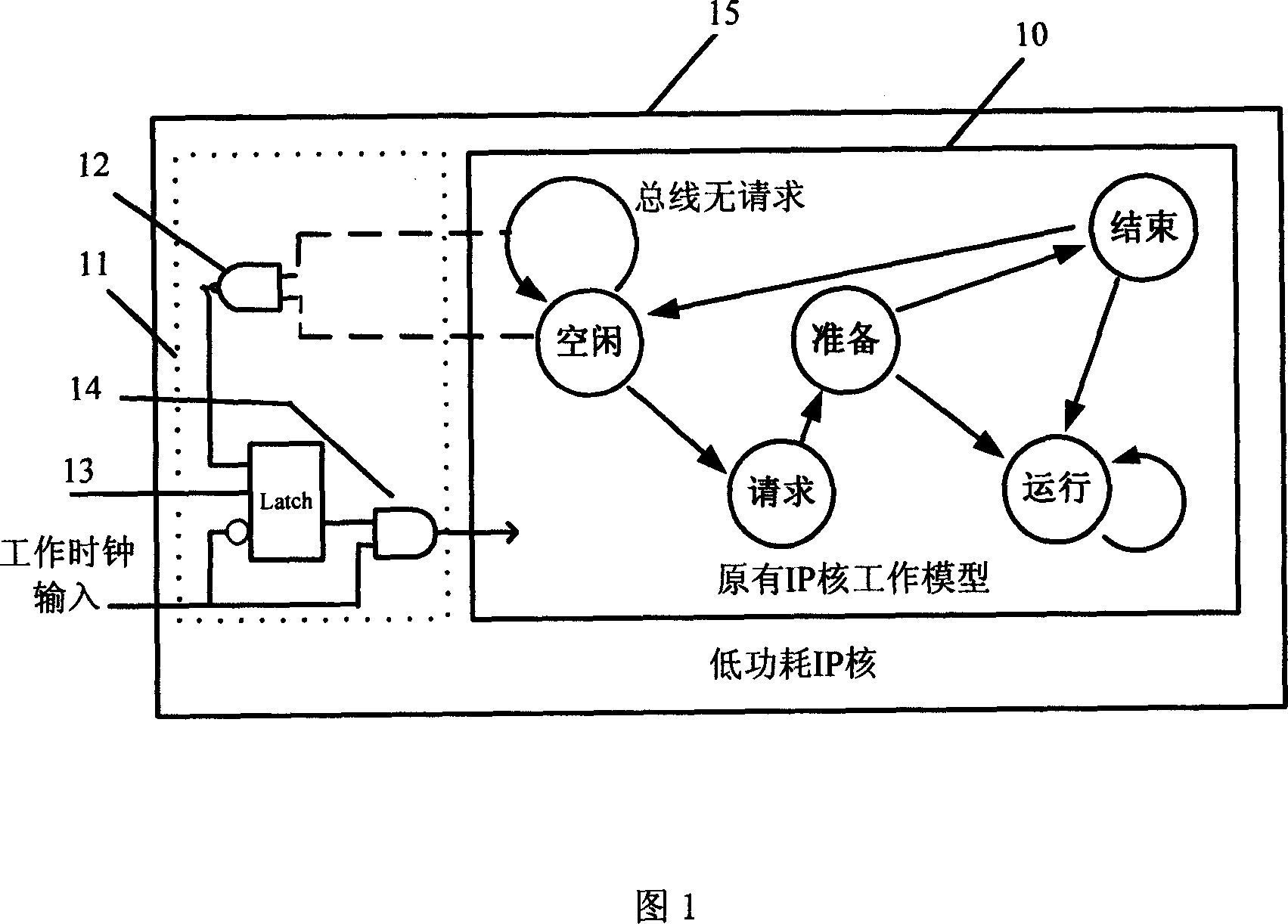
[0025] As shown in FIG. 1 , this embodiment describes a schematic diagram of reducing power consumption of the original IP core in an explicit state.
[0026] Step a) Divide all the states of the original IP core into two categories - "idle" state and "working" state, the "working" state is not the "idle" state, and the "idle" state means that the IP core is not currently working effectively status. details as follows:
[0027] Among the figure, the working model of the original IP core 10 is in the box, and the state of the original IP core 10 has "idle", "request", "ready", "running", "end"; when in the "idle" state, If the bus has no request, it remains in the "idle" state, and if the bus sends a request, it enters the "running" state; the circle in the figure indicates the state, and the arrow indicates the transition, indicating the next state of the state machine. The state in the actual circuit of the original IP core 10 is realized by a series of registers (sequentia...
Embodiment 2
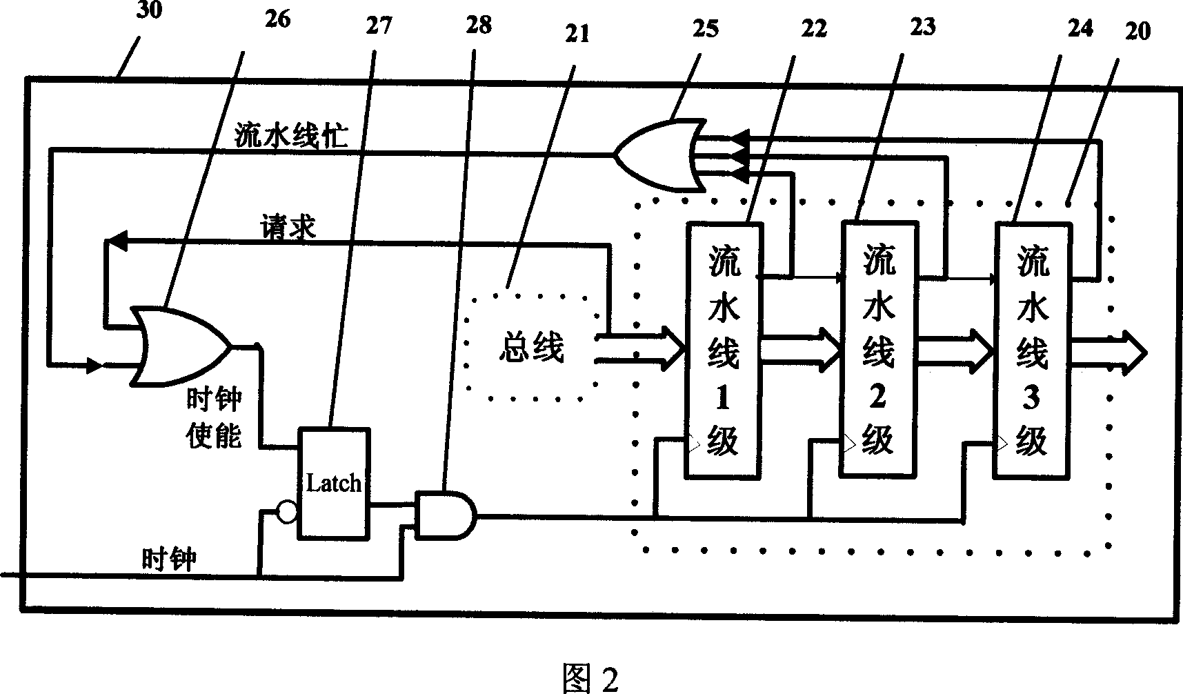
[0037] FIG. 2 is a schematic diagram of reducing power consumption of the original IP core described in an implicit state according to another embodiment of the present invention, illustrating a specific method for low power consumption modification. The original design pipeline of this IP core is divided into three pipelines, and each level is a register slot containing many register bits. The method for reducing power consumption in this embodiment includes:
[0038] Step a) Divide all the states of the original IP core into two categories - "idle" state and "working" state, the "working" state is not the "idle" state, and the "idle" state means that the IP core is not currently working effectively status.
[0039] The original IP core of this embodiment is different from most IP cores in that there is no explicit state machine description in the design code described by the hardware description language, and its state is implicitly represented by the effective bits of the ...
PUM
 Abstract
Description
Claims
Application Information