Substrate processing method and substrate processing apparatus
A substrate processing method and a substrate processing device technology, which are applied in the direction of electrical components, semiconductor/solid-state device manufacturing, circuits, etc., can solve the problems of substrate pollution, collapse, and time spent on rinsing, and achieve the effect of preventing pattern collapse
- Summary
- Abstract
- Description
- Claims
- Application Information
AI Technical Summary
Problems solved by technology
Method used
Image
Examples
no. 1 approach
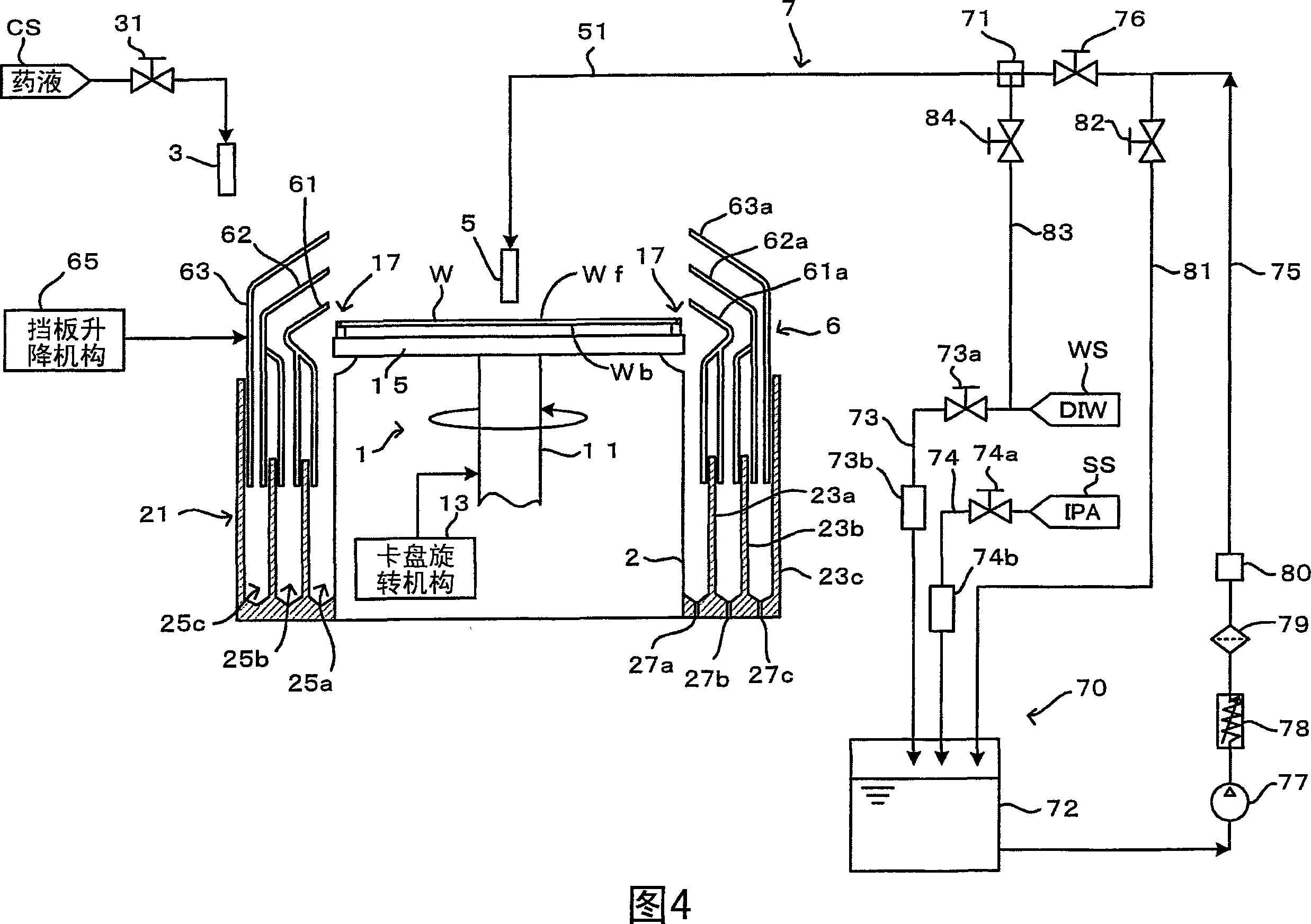
[0062] FIG. 4 is a diagram showing a first embodiment of the substrate processing apparatus of the present invention. In addition, FIG. 5 is a block diagram showing a control structure of the substrate processing apparatus of FIG. 4 . This substrate processing apparatus is a single-sheet substrate processing apparatus for cleaning processing for removing contaminants adhering to the surface Wf of a substrate W such as a semiconductor wafer. Specifically, this is an apparatus in which chemical solution treatment with a chemical solution such as hydrofluoric acid and pure water or After the rinsing treatment with rinsing solution such as DIW, the substrate W wetted with the rinsing solution is subjected to a replacement treatment described later, and then the substrate W is subjected to drying treatment.
[0063] This substrate processing apparatus includes: a spin chuck 1 that rotates the substrate while holding the substrate in a substantially horizontal posture with its surf...
no. 2 approach
[0101] FIG. 10 is a diagram showing a second embodiment of the substrate processing apparatus of the present invention. In addition, FIG. 11 is a block diagram showing a control structure of the substrate processing apparatus of FIG. 10 . The substrate processing apparatus of the second embodiment differs greatly from the first embodiment in that a blocking member 9 functioning as an "environment blocking device" of the present invention is provided above the spin chuck 1 . In addition, since other structures and operations are basically the same as those of the first embodiment, the same reference numerals are assigned here, and descriptions thereof are omitted.
[0102] The blocking member 9 is a disk-shaped member having an opening at the center, and is positioned above the spin chuck 1 . The lower surface (bottom surface) of the blocking member 9 is formed as an opposing surface substantially parallel to the substrate surface Wf, and its planar size is formed to be larger...
no. 3 approach
[0111] 12A, 12B, and 12C are diagrams showing a third embodiment of the substrate processing apparatus of the present invention. A significant difference between the substrate processing apparatus of the third embodiment and the first and second embodiments is that a pre-drying process is performed after the replacement process and before the drying process. In addition, since the other configurations and operations are basically the same as those of the second embodiment, the same reference numerals are assigned here, and description thereof will be omitted.
[0112] In this embodiment, after the replacement with the mixed solution (replacement step) and before the substrate W is dried (drying step), a drying pretreatment step as described below is performed. First, the liquid mixture is supplied to the substrate surface Wf to form the liquid mixture layer 21 in the liquid immersion state on the entire substrate surface ( FIG. 12A ). Next, nitrogen gas is sprayed from the ga...
PUM
| Property | Measurement | Unit |
|---|---|---|
| surface tension | aaaaa | aaaaa |
Abstract
Description
Claims
Application Information


