Semiconductor device

A technology for semiconductors and devices, applied in the field of semiconductor devices, can solve the problems of increasing the area of ​​ESD protection circuits, the cost of ESD protection circuits, etc.

Inactive Publication Date: 2008-01-02
RICOH KK
View PDF1 Cites 3 Cited by
  • Summary
  • Abstract
  • Description
  • Claims
  • Application Information

AI Technical Summary

Problems solved by technology

However, these proposals require additional circuits such as inverters, and increase the area occupied by the ESD protection circuit and the cost of the ESD protection circuit

Method used


Image

  • Semiconductor device
  • Semiconductor device
  • Semiconductor device

Examples


Embodiment Construction

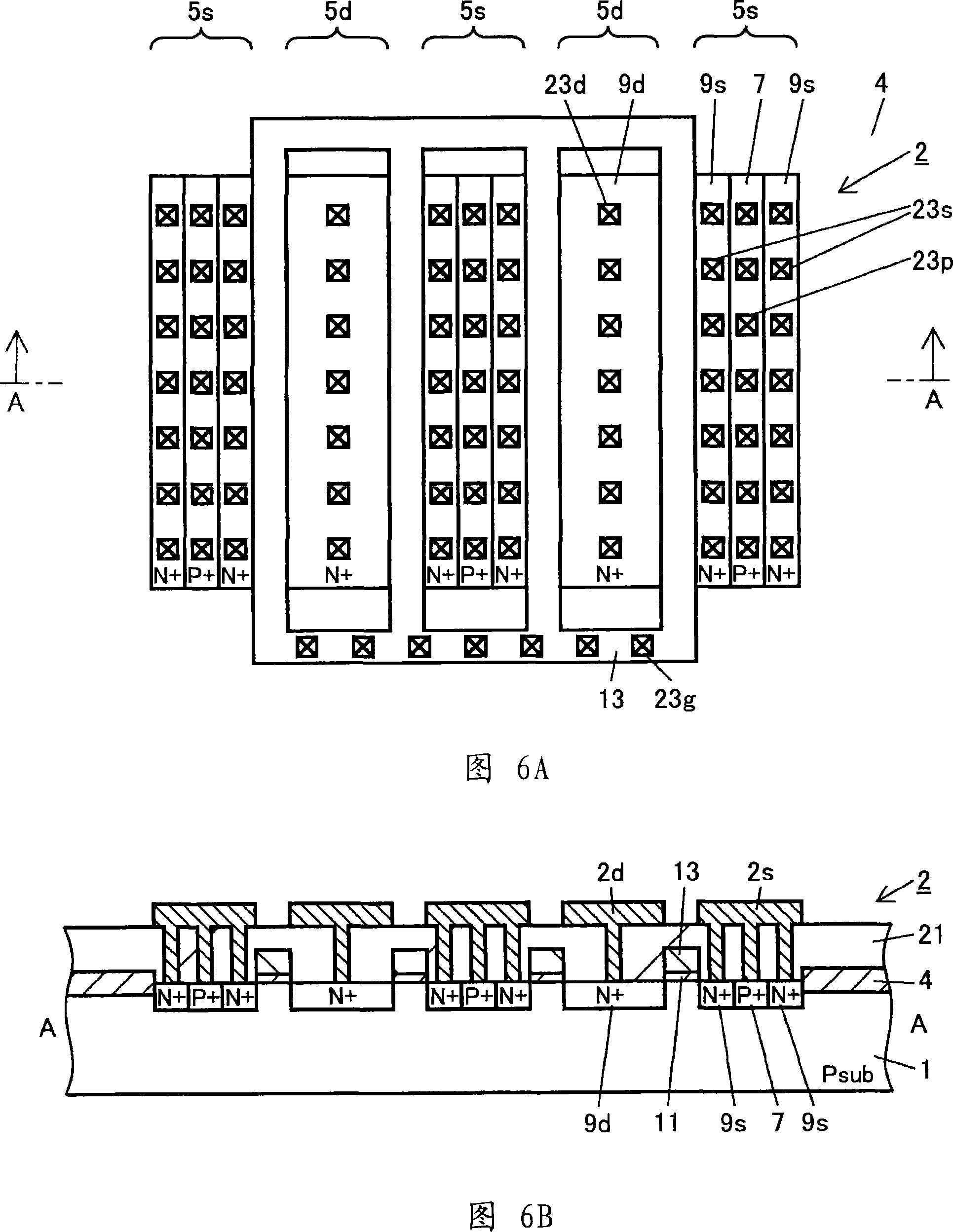
[0033] 6A to 6D are diagrams showing a first embodiment of a semiconductor device according to the present invention. 6A is a plan view showing an output NMOS driver, and FIG. 6B is a cross-sectional view of the output NMOS driver taken along line A-A of FIG. 6A. FIG. 6C is a plan view of a grounded gate NMOS (ggNMOS) protection element, and FIG. 6D is a cross-sectional view of the ggNMOS protection element taken along line B-B of FIG. 6C . FIG. 7 is a circuit diagram showing a first embodiment of the semiconductor device. First, a description will be given of the structures of the output NMOS driver and the ggNMOS protection element with reference to FIGS. 6A to 6D .

[0034] The LOCOS oxide layer 4 is formed on the P-type silicon substrate 1 to define a driver formation area where an output NMOS driver (NMOS switching element) 2 is formed and a protection element formation area where a ggNMOS protection element (NMOS protection element) 3 is formed.

[0035] A description ...


PUM


Abstract

A semiconductor device includes an NMOS switching element having an N-type drain diffusion region coupled to an input and / or output terminal, and an N-type source diffusion region and a P-type substrate contact diffusion region coupled to a ground line; and an NMOS protection element having an N- type drain diffusion region coupled to the input and / or output terminal, and a gate, an N-type source diffusion region and a P-type substrate contact diffusion region coupled to the ground line, wherein the N-type source diffusion region and the P-type substrate contact diffusion region of the NMOS switching element are arranged adjacent to each other, and the N-type source diffusion region and the P-type substrate contact diffusion region of the NMOS protection element are arranged with a spacing therebetween. If the N and P types are interchanged, the ground line is replaced by a power supply line.

Description

technical field [0001] The present invention generally relates to semiconductor devices, and more particularly, to a semiconductor device having a switching element composed of a metal oxide semiconductor (MOS) transistor and a protection element composed of the MOS transistor for protecting the switching element. Background technique [0002] 1 and 2 are circuit diagrams for explaining a general electrostatic discharge (ESD) protection circuit of an output terminal. FIG. 1 shows a CMOS type ESD protection circuit, and FIG. 2 shows an NMOS open-drain type ESD protection circuit. The ESD protection circuit shown in FIG. 1 has a local clamp circuit (clamp) 101, a PMOS transistor 102, an NMOS transistor 103, an output terminal OUT, a power supply terminal VDD, and a ground terminal GND. The ESD protection circuit shown in FIG. 2 has a local clamp circuit 101, an NMOS transistor 104, an output terminal OUT, and a ground terminal GND. [0003] FIG. 3 is a circuit diagram showin...

Claims


Application Information

Patent Timeline
Patent Type & Authority Applications(China)
IPC IPC(8): H01L27/06H01L21/822H01L21/8238H01L27/04H01L27/092
CPCH01L27/088H01L27/092H01L27/0266
Inventor 桥上裕幸
Owner RICOH KK
Why Eureka
Try Eureka