Liquid crystal display panel and method for producing same, device comprising same

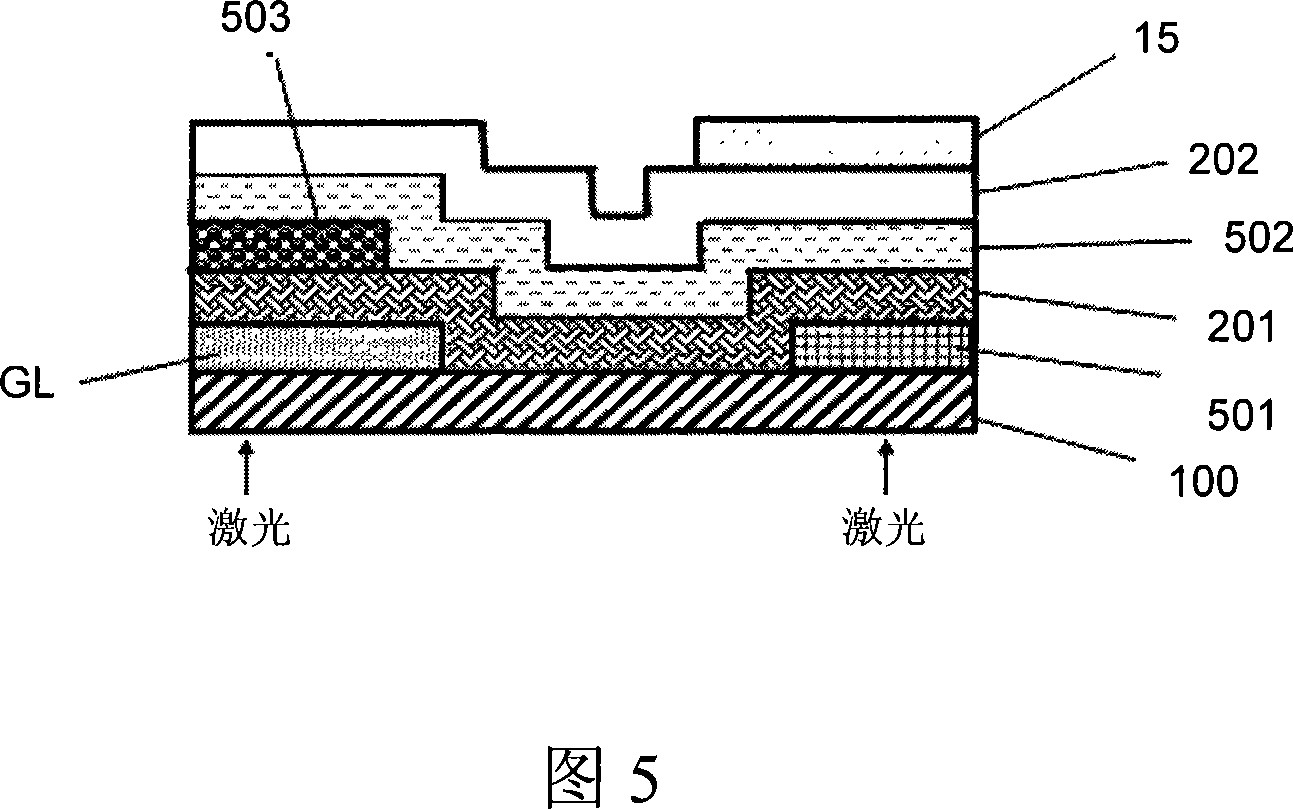
A liquid crystal display panel and substrate technology, applied in nonlinear optics, instruments, optics, etc., can solve the problems of easily burnt pixel electrodes, unable to repair bright spot defect pixels, difficult to control the temperature of laser beam heating, etc., to reduce the heating temperature , Prevent the effect of overheating

Active Publication Date: 2008-01-16
KUSN INFOVISION OPTOELECTRONICS
View PDF1 Cites 5 Cited by
  • Summary
  • Abstract
  • Description
  • Claims
  • Application Information

AI Technical Summary

Problems solved by technology

[0007] In the above method, since the temperature heated by the laser beam is often difficult to control, when the temperature is too high, the heat generated can easily burn out the pixel electrodes, resulting in the inability to repair bright defect pixels into dark defect pixels

Method used


Image

  • Liquid crystal display panel and method for producing same, device comprising same
  • Liquid crystal display panel and method for producing same, device comprising same
  • Liquid crystal display panel and method for producing same, device comprising same

Examples


Embodiment Construction

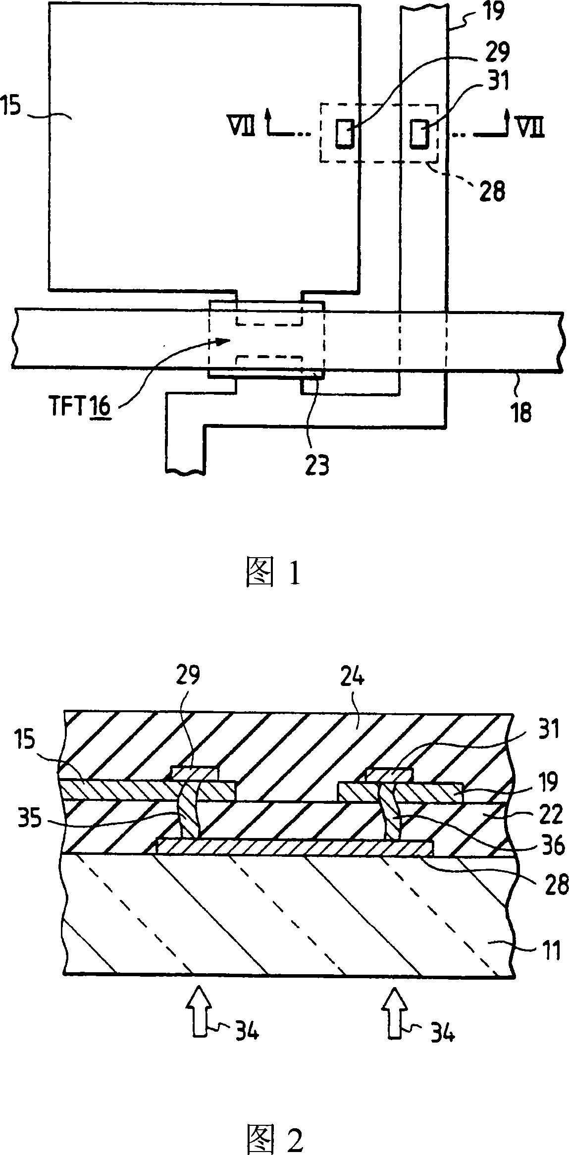
[0029] The following detailed description sets forth some exemplary embodiments of the invention by way of illustration only. As those skilled in the art will realize, the present invention can be applied in many different ways and should not be limited to the embodiments set forth herein. In addition, in the present invention, when a certain layer is referred to as being located or disposed between two other layers, it should be broadly understood that the layer can either directly border on the other two layers, or be connected to the other two layers through other layers. The two floors are separated.

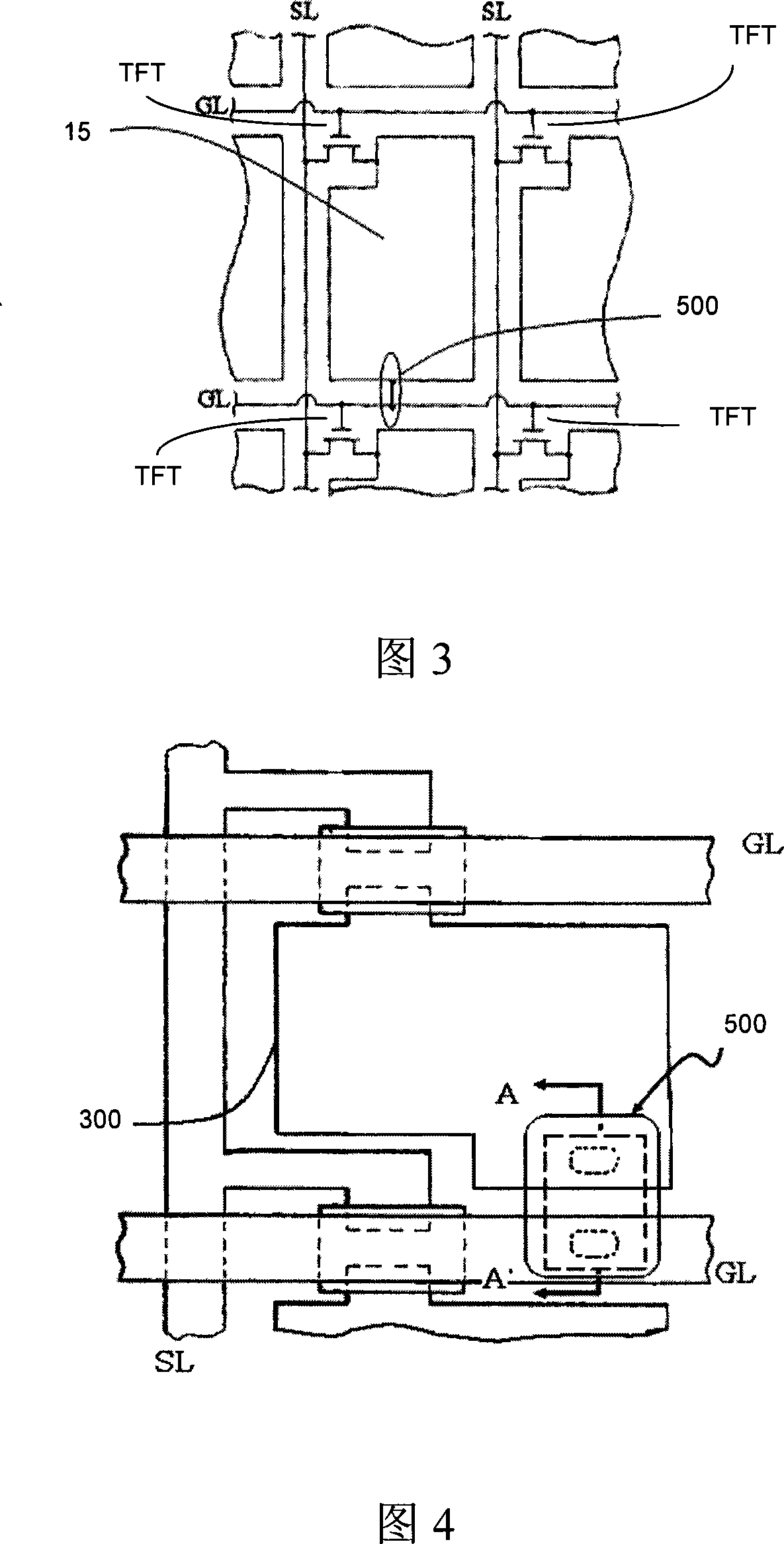
[0030] FIG. 3 is a schematic plan view of a pixel array substrate of a typical liquid crystal display panel. The pixel array of the liquid crystal display panel is formed on a substrate (not shown), and as shown in FIG. The pixel electrodes 15 near the area and the thin film transistors TFT that connect each pixel electrode 15 with the gate line and the data line, wherein ...


PUM


Abstract

The invention provides a liquid crystal display panel which comprises a base board, data lines and gate lines both of which are reciprocal cross and forms on the base board and a pixel electrode equipped on the cross area of the data lines and the gate lines; the liquid crystal further comprises a conducting layer which comprises the overlap part of the pixel electrode in space and the overlap part of the gate lines or data lines in space and a first cushioning layer which is equipped between the base board and the pixel electrode and is used to weaken the energy of light beam. When the invention implements laser mend to the light spot defect if the liquid crystal display panel, the first cushion layer can effectively absorb one part of energy of laser beam, which hence reduces the heating temperature of the laser beam and prevents the elements such as the pixel electrode from being burned out because of too high temperature of the elements.

Description

technical field [0001] The invention relates to a liquid crystal display technology, in particular to a liquid crystal display panel with a laser repair function and a manufacturing method thereof, a liquid crystal display including the panel, a portable electronic device and a method for repairing point defects of the liquid crystal display panel. Background technique [0002] Liquid crystal display panels can be divided into two types: active matrix type and passive matrix type, according to their working methods. The active liquid crystal display panel is composed of millions of transistors, and the corresponding pixels are controlled by the transistors to turn on and off. However, in the manufacturing process of the active liquid crystal display panel, point defects often occur due to reasons such as manufacturing errors. Point defects generally have two forms: bright point defects and dark point defects. Normally, the human eye is more sensitive to bright spot defects...

Claims


Application Information

Patent Timeline
Patent Type & Authority Applications(China)
IPC IPC(8): G02F1/13G02F1/1362
CPCG02F1/136259G02F2001/136268G02F2201/508G02F1/136268
Inventor 钟德镇乔艳冰
Owner KUSN INFOVISION OPTOELECTRONICS
Why Eureka
Try Eureka