Circuit board element and welding flux separating and recovery method and device thereof

A technology for separation and recovery of circuit boards, applied in auxiliary devices, welding equipment, manufacturing tools, etc., can solve problems such as volatilization or oxidation of circuit boards, large consumption of hot air, damage to the shape of components, etc., to achieve complete separation of solder, The effect of low energy consumption and small thermal shock

Inactive Publication Date: 2008-01-30
SICHUAN CHANGHONG ELECTRIC CO LTD
View PDF6 Cites 49 Cited by
  • Summary
  • Abstract
  • Description
  • Claims
  • Application Information

AI Technical Summary

Problems solved by technology

[0011] 1. By heating the circuit board as a whole until the solder melts, the components are placed in a high-temperature (over 180°C) environment for a long time, and the components are subjected to a large thermal shock, which increases the possibility of component failure, and the separated components Device performance is low
In addition, the toxic elements in the circuit board may volatilize or oxidize under continuous high temperature, emitting toxic and harmful substances such as dioxin, polluting the environment
[0012] 2. After the components are disassembled, some heating medium adheres to the components and solder, which becomes a new impurity introduced during the disassembly process, which affects the reuse of components and reduces the purity of the recycled solder
[0013] 3. Solder separation is not complete
[0015] 5. During the disassembly process, the violent collision between the components and the recycling device, as well as operations such as sweeping, scraping, cutting, and hitting on the pins of the components, will damage the appearance of the components and affect the reuse of components
[0016] 6. The disassembly method disclosed in the patent application of Tsinghua University is adopted. Due to the unreasonable structure of the hot air nozzle and the unreasonable assembly position, the consumption of hot air is large, the energy consumption is high, and the effect of separating solder and components is very poor.

Method used


Image

  • Circuit board element and welding flux separating and recovery method and device thereof
  • Circuit board element and welding flux separating and recovery method and device thereof

Examples


Embodiment

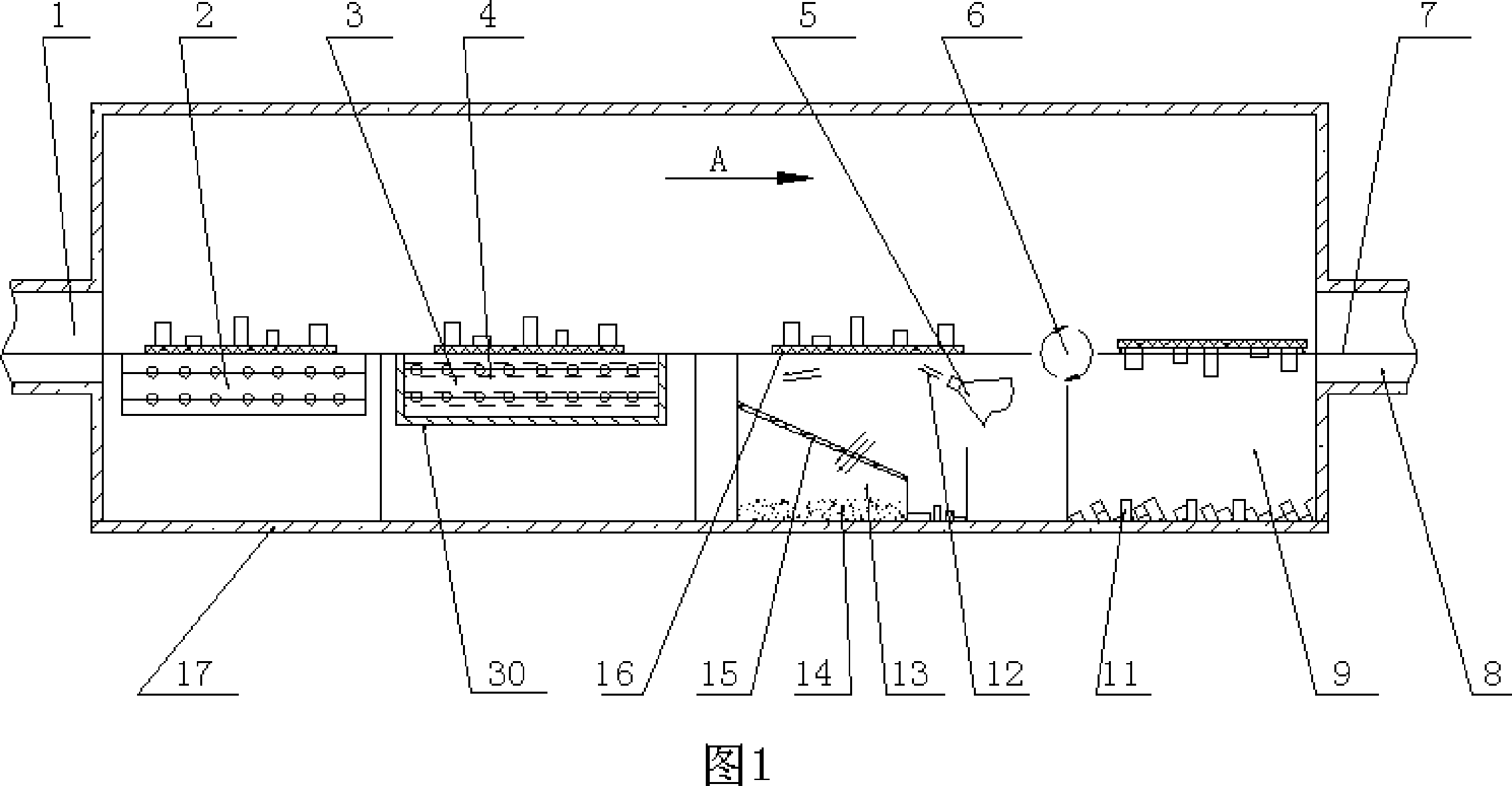
[0055] Referring to Fig. 1, after the circuit board 16 to be disassembled is clamped and fixed, it is transported to the preheating device 2 by the clamping and conveying mechanism 7 through the entrance 1 of the heat preservation chamber, and the whole is heated by the combination of the resistance wire or the infrared heating plate in the preheating device 2 and the hot air. The circuit board is preheated to 140-180°C.

[0056] The preheated circuit board 16 is sent to the heating device 3 to heat the circuit board 16 . The heating device 3 is composed of a solder melting tank 30 placed below the clamping and conveying mechanism 7. The molten solder 4 in the solder melting tank 30 is in contact with the soldering surface of the circuit board 16, and the soldering surface of the circuit board 16 is heated until the solder melts.

[0057] The heating method refers to the heating and welding process in the wave soldering process. The preheated circuit board 16 is passed throug...


PUM

PropertyMeasurementUnit
distanceaaaaaaaaaa

Abstract

The invention relates to recycle and reuse technology of electronic castoff, in particular to a method and a device to remove the element and separate the welding material from the circuit board. The invention discloses the method and the device which separates and recycles the welding material and removes the elements on the circuit board with high efficiency. The technic proposal of the invention adopts the melting welding material as the heating medium and heats the welding pots on the welding surface of the circuit board; the welding material is separated from the circuit board by utilizing the special nozzle to spray high-temperature high-pressure gas; finally, the circuit board is turned over and vibrated, separating the element from the circuit board. The invention has the beneficial effects that the element is subject to small heat impact during the removal process, the element after removal has high intact rate and repeated ratio, and the new impurity is not brought in during the removal process. The invention has the advantages of complete separation of welding pot, high removal ratio of elements, low energy consumption, environment-friendship, etc.

Description

technical field [0001] The invention relates to the recycling technology of electronic waste, in particular to a method and device for disassembling components and separating solder from a circuit board. Background technique [0002] The circuit board is generally a printed circuit board (Printed Circuit Board, referred to as PCB). Commonly referred to as a circuit board, it is mainly composed of components, printed circuit board substrates, and solder connecting components and printed circuit board substrates. It is the most basic and important component of electronic and electrical equipment such as televisions, air conditioners, computers, monitors, and fax machines. part. In recent years, electronic and electrical equipment, especially consumer electronic products, have developed rapidly and are frequently updated. More and more electronic and electrical equipment are discarded due to the end of their service life or replacement. As an important part of electronic and ...

Claims


Application Information

Patent Timeline
Patent Type & Authority Applications(China)
IPC IPC(8): B23K1/018B23K1/20B23K3/08B09B5/00
Inventor 潘晓勇李中良郅慧王炼
Owner SICHUAN CHANGHONG ELECTRIC CO LTD
Why Eureka
Try Eureka