
Super resolution lithography method based on PDMS template and silver board material

A super-resolution and silver plate technology, applied in photosensitive materials for optomechanical equipment, micro-lithography exposure equipment, metal material coating technology, etc., can solve problems such as photolithography technology that is difficult to batch nanoscale structure photolithography , to achieve the effect of improving the lithography resolution and simplifying the complexity

Inactive Publication Date: 2008-02-20
INST OF OPTICS & ELECTRONICS - CHINESE ACAD OF SCI
View PDF0 Cites 9 Cited by
  • Summary
  • Abstract
  • Description
  • Claims
  • Application Information

AI Technical Summary

Problems solved by technology

[0004] The technical problem to be solved by the present invention is to provide a super-resolution photolithography method based on PDMS templates and silver plate materials, which realizes practical The batch production of micro-nano structures is suitable for the preparation of various scale structures from tens of nanometers to millimeters, which not only greatly improves the resolution, but also reduces the complexity of traditional photolithography

Method used


Image

  • Super resolution lithography method based on PDMS template and silver board material
  • Super resolution lithography method based on PDMS template and silver board material

Examples


Embodiment Construction

[0033] The present invention will be described in detail below in conjunction with specific embodiments, but the scope of protection of the present invention is not limited to the following examples, and should include all content in the claims.

[0034] The metal types in the present invention (such as metal gold, silver, aluminum, etc.) all have the same effect, and the target micro-nano structures of different materials chromium, or gold, or silver, or copper in the steps all have the same processing technology , and the choice of infrared material and visible light material for the base material in the present invention also have the same process steps, so the present invention only gives an example, and other implementation modes are completely similar to this example.

[0035] Concrete steps of the present invention are as follows:

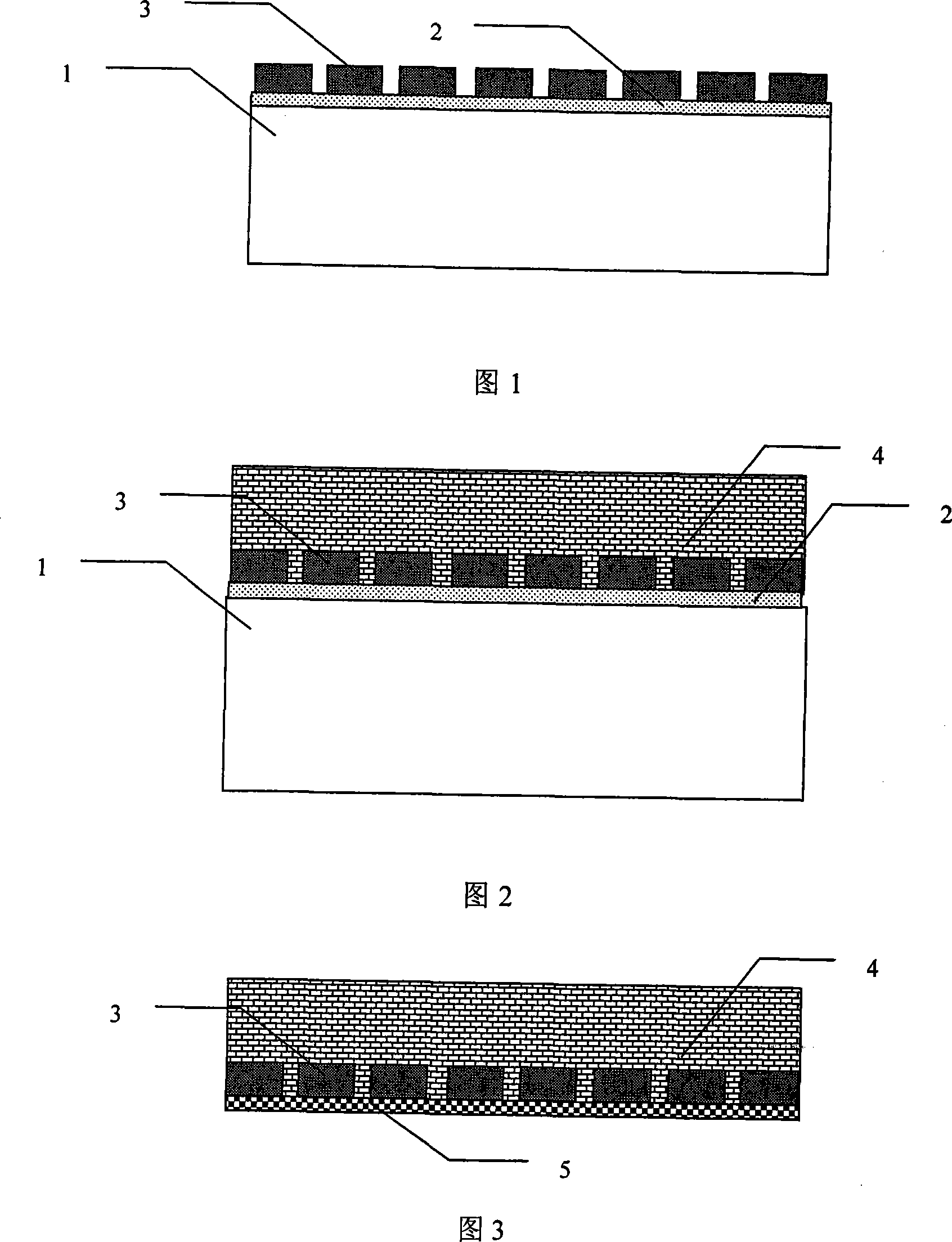
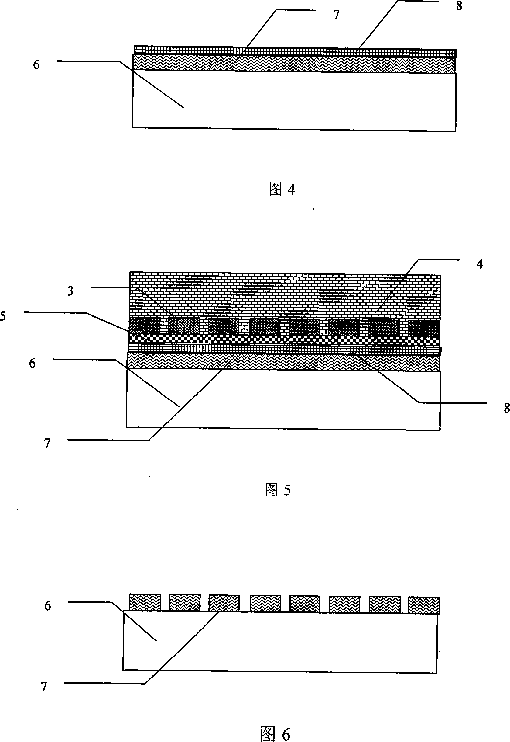
[0036] (1) First select the quartz material 1 as the base material, vapor-deposit a 10nm metal gold film 2 on the surface of the quartz mat...


PUM


Abstract

The utility model relates to a super-resolution photolithography method based on the PDMS template and the silver plate material, which comprises the following steps: a metallic film layer which has week adhering capability on a base is vapor-plated on the surface of the base; a micro-nano target structure is produced on the metallic film surface; after mixed with the curing agent, the PDMS is cast on the surface of the metallic film layer; the mixture is solidified in the environment with temperature of 25 to 95 DEG C to generate an elastic film; the PDMS film is lifted and the metallic film layer adhered on the surface of the PDMS film is removed, and then the micro-nano target structure is embedded in the PDMS film; a protective layer with the thickness of 10 to 100nm is spin-coated on the PDMS surface to form a super-resolution photoetching mask; the photoresist is spread on the surface of another substrate, on which a silver layer with the thickness of 10 to 100nm is vapor-plated; the figure surface of the super-resolution photoetching mask is accurately attached with the silver layer on the photoresist surface and then the super-resolution photoetching mask and the silver film are removed through exposure, and the photoresist is developed; and then the required target figure is formed. The utility model not only improves the resolution greatly, decreases the complexity of the traditional photolithography method, but also utilizes the elasticity of the PDMS material and realizes the micro-nano structure molding on the curved surface of the material.

Description

technical field [0001] The invention belongs to the technical field of micro-nano structure processing, in particular to a super-resolution photolithography method based on a PDMS template and a silver plate material. Background technique [0002] In recent years, with the rapid development of micro-nano processing technology and nanomaterials, the electromagnetic properties of micro-nano metal structures are receiving more and more attention. The interaction of light with surface micro-nano metal structures produces a series of new and exotic physical phenomena. For example, in 1998, French scientist Ebbesen and his collaborators discovered the phenomenon of extraordinary enhancement (Extraordinary Optical Transmission) of light passing through a subwavelength metal hole array. The research of H.J.Lezec et al. further showed that: when the light passes through the sub-wavelength metal nanohole, its transmittance can not only be enhanced, but also the diffraction angle of t...

Claims


Application Information

Patent Timeline
IPC IPC(8): G03F7/00G03F7/004G03F7/20B81C1/00
Inventor 杜春雷罗先刚董小春刘强
Owner INST OF OPTICS & ELECTRONICS - CHINESE ACAD OF SCI
Learn More