Gate driver for outputting superposition-free scanning signal, liquid crystal display and method

A gate driver and scanning signal technology, applied to static indicators, instruments, etc., can solve the problems of complex signal blocking circuit design, difficulty in streamlining the manufacturing process and saving costs, and achieve improved picture quality, cost savings, and streamlined manufacturing The effect of the process

Active Publication Date: 2008-02-20
AU OPTRONICS CORP
View PDF4 Cites 16 Cited by
  • Summary
  • Abstract
  • Description
  • Claims
  • Application Information

AI Technical Summary

Problems solved by technology

However, the design of the signal blocking circuit disclosed in the aforementioned patents and patent application publications is relatively complex, including multiple complex logic switch circuits, so it is impossible to implement the design with a single active component of NMOS or PMOS architecture, and it is difficult to achieve simplified manufacturing Process and Cost Saving Targets

Method used


Image

  • Gate driver for outputting superposition-free scanning signal, liquid crystal display and method
  • Gate driver for outputting superposition-free scanning signal, liquid crystal display and method
  • Gate driver for outputting superposition-free scanning signal, liquid crystal display and method

Examples


Embodiment Construction

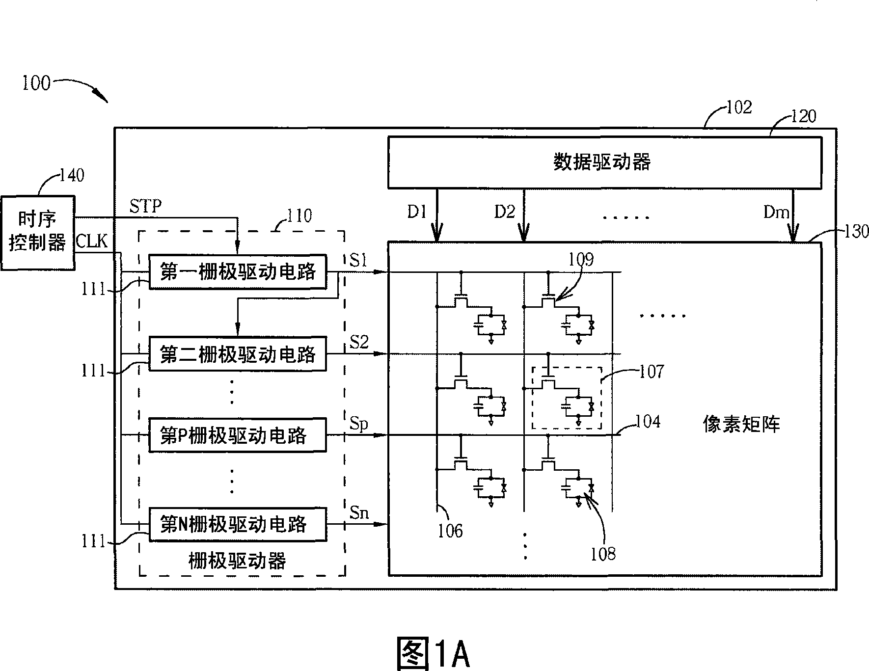
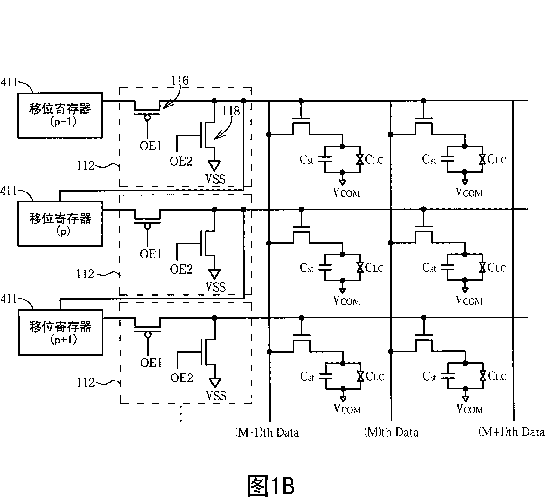
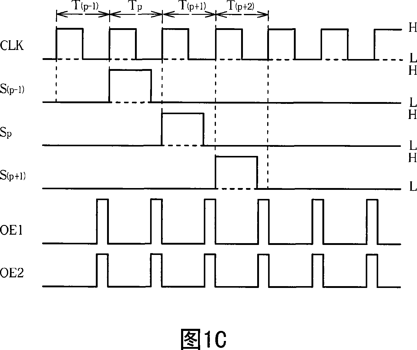
[0051] Please refer to FIG. 1A , which is a structural block diagram of the first embodiment of the liquid crystal display of the present invention. The liquid crystal display 100 includes a substrate 102, a pixel matrix 130, a gate driver 110, a data driver 120 and a timing controller 140, wherein the peripheral circuit design of the liquid crystal display 100 is mainly a CMOS structure, and the thin film transistor of the pixel matrix 130 is The NMOS structure is disposed on the substrate 102 . The pixel matrix 130 includes a plurality of gate lines 104 , a plurality of data lines 106 , a plurality of pixels 107 and a pixel capacitor 108 . Both the gate lines 104 and the data lines 106 are arranged on the substrate 102 , and they are interlaced with each other. Each pixel 107 includes a thin film transistor 109 coupled to a gate line 104 and a data line 106 . The pixel capacitor 108 is coupled to the thin film transistor 109 . The gate driver 110 includes N-level gate dri...


PUM


Abstract

The utility model provides an associated grid driver and method, and an LCD (liquid crystal display) outputting zero overlapping scanning signals, comprising multilevel grid drive circuits, wherein, the grid drive circuits are coupled with each other, and used to output a plurality of scanning signals; each level of grid drive circuit comprises a shift register and an obstruction circuit, wherein, the shift register is used to generate a scanning signal in light of a frequency signal and the scanning signals of a previous grid driver circuit; the obstruction circuit is coupled with the shift register, and used to block the scanning signals output by the shift register for a pre-arranged period, so as to generate a plurality of scanning signals without overlapping time sequences between the adjacent levels of the grid drive circuits, and improve image qualities of the LCD (liquid crystal display).

Description

technical field [0001] The invention relates to a liquid crystal display and a driving circuit, in particular to a barrier circuit and a timing control method in a gate driver (Gate Driver). Background technique [0002] FIG. 4A is a structural block diagram of a conventional liquid crystal display. Referring to FIG. 4A , the liquid crystal display 400 includes a gate driver 410 , a data driver (Data Driver) 420 , a pixel matrix (PixelMatrix) 430 and a timing controller (Timing Controller) 440 . The pixel matrix 430 includes a plurality of gate lines 104 , a plurality of data lines 106 , a plurality of pixels 107 and pixel capacitors 108 . The gate lines 104 and the data lines 106 are arranged on the substrate 402 and intersect with each other. Each pixel 107 includes a thin film transistor 109 coupled to the gate line 104 and the data line 106 . The pixel capacitor 108 is coupled to the thin film transistor 109 . The gate driver 410 includes a first shift register 411 ,...

Claims


Application Information

Patent Timeline
Patent Type & Authority Applications(China)
IPC IPC(8): G09G3/36G09G3/20G02F1/133
Inventor 刘斡中
Owner AU OPTRONICS CORP
Why Eureka
Try Eureka