Semiconductor device and fabrication process thereof
A semiconductor and device technology, applied in the field of semiconductor devices with multi-layer interconnection structure and its manufacturing, can solve problems such as film peeling and short circuit
- Summary
- Abstract
- Description
- Claims
- Application Information
AI Technical Summary
Problems solved by technology
Method used
Image

Examples
no. 1 example
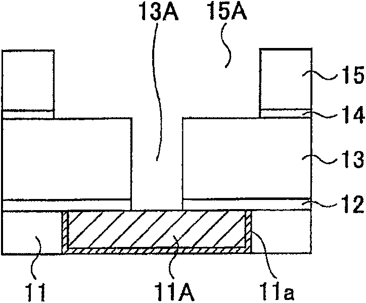
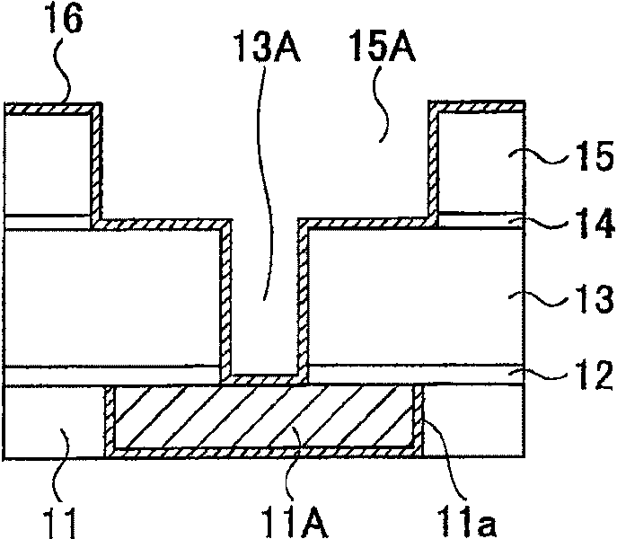
[0073] Figure 8A to Figure 8E It is a schematic diagram illustrating a method for manufacturing a semiconductor device with a multilayer interconnection structure according to the first embodiment of the present invention.
[0074] refer to Figure 8A , active devices (not shown) such as transistors are formed on the silicon substrate 21, and the silicon substrate 21 is covered with an insulating film 21A.
[0075] On the insulating film 21A, an interlayer insulating film 23 in which interconnections such as Cu are embedded via a barrier metal film 23a such as Ta is formed via an etching stopper film 22 such as SiC or SiN. Even pattern 23A.
[0076] On the interlayer insulating film 23 , the next interlayer insulating film 25 having a thickness of 200 nm is formed via, for example, an etching stopper film 24 (for example, 50 nm in thickness) of SiC, SiN, or the like.
[0077] For the interlayer insulating films 23, 25, and 27, low-K dielectric films of inorganic or organic...
no. 2 example
[0097] At the same time, in progress Figure 8B The film thickness of the barrier metal film 28 required to protect the bottom of the interconnection groove 27A at the second step of the bias sputtering process shown and thereafter when the sputtering-etching process is performed varies with the sputtering-etching process. The Vd / Ve ratio during the etching process varies. Therefore, in this case, in the first step, barrier metal film 28 having a larger thickness is formed at the bottom of interconnection groove 27A.
[0098] Also, in the second step, a Vd / Ve ratio whose value is much smaller than 1.0 may be used.
[0099] Therefore, in this case, compared with the previously described embodiment, it is possible to increase Figure 8B The amount of etching in the second step is shown.
[0100] On the other hand, in the case where the barrier metal film 28 formed on the bottom of the interconnection trench 27A has a small film thickness, according to the previous embodiment,...
PUM
 Abstract
Description
Claims
Application Information
 - R&D
- Intellectual Property
- Life Sciences
- Materials
- Tech Scout
- Unparalleled Data Quality
- Higher Quality Content
- 60% Fewer Hallucinations
Browse by: Latest US Patents, China's latest patents, Technical Efficacy Thesaurus, Application Domain, Technology Topic, Popular Technical Reports.
© 2025 PatSnap. All rights reserved.Legal|Privacy policy|Modern Slavery Act Transparency Statement|Sitemap|About US| Contact US: help@patsnap.com