A micron wave length THz radiation transmission chip and its making method

A technology of radiation emission and manufacturing method, which is applied in the micron-wavelength THz radiation emission chip and its manufacturing field, and can solve the problems of high cost, low output power, and limited system development of titanium sapphire femtosecond lasers.

Inactive Publication Date: 2008-03-26
INST OF SEMICONDUCTORS - CHINESE ACAD OF SCI
View PDF0 Cites 9 Cited by
  • Summary
  • Abstract
  • Description
  • Claims
  • Application Information

AI Technical Summary

Problems solved by technology

However, the Ti:Sapphire femtosecond laser itself is expensive and the output power is small, which limits the development of the system

Method used


Image

  • A micron wave length THz radiation transmission chip and its making method

Examples


example

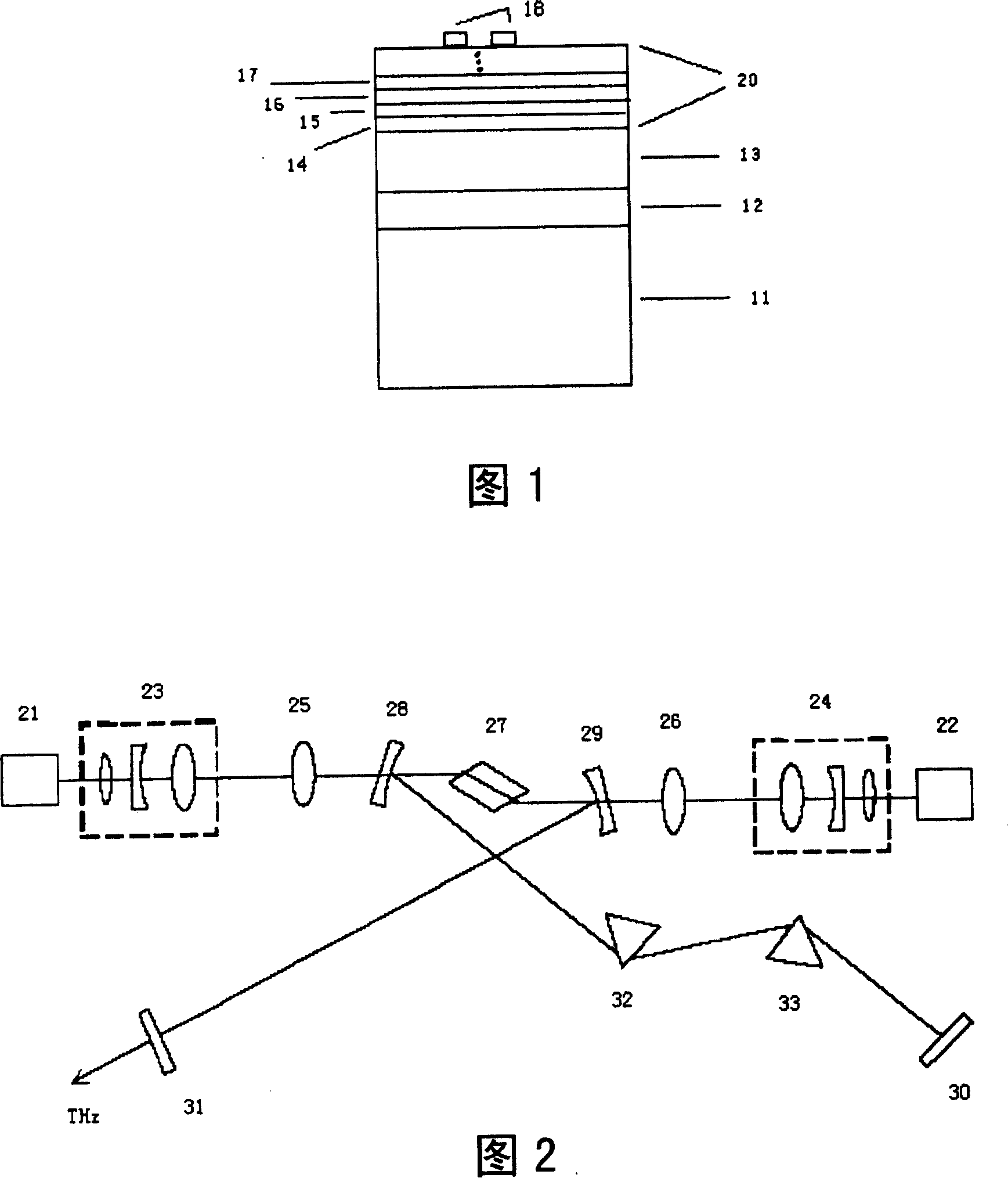
[0056] Please refer to FIG. 1 , the present invention proposes a manufacturing method of a THz radiation emitting chip suitable for low-temperature growth of InGaAs thin films excited by a femtosecond laser with a wavelength of one micron combined with Bragg reflectors for electric field bias. The device adopts n+GaAs substrate 11 as the substrate material for epitaxial growth. First grow a 200nm-500nm buffer layer 12 on an n+GaAs substrate 11, then grow a Bragg mirror 13, and then grow 5-10 pairs of quantum wells 20, each pair of quantum wells includes GaAs 1 4 / Ga 0.5As 0.5P 1 5 / In O.25 Ga 0.75 As 16 / GaAs 1 7. The thickness of GaAs 1 4 and GaAs 1 7 is generally 15nm-25nm, Ga 0.5As 0.5P 1 5 is the strain compensation area, the thickness is generally 10nm-12nm, In 0.25 Ga 0.75 As 1 5 is the light absorption area, the thickness is generally 8nm -10nm. The quantum well 20 is a carrier relaxation region, which is grown at a low temperature, and the growth temperature is 500°C-5...


PUM


Abstract

This invention relates to a THz radiation chip of one micron wave length including: a substrate, a buffer layer prepared on the substrate, a Bragg reflection mirror set on the buffer layer to form a reflection mirror of high reflection rate and multiple quantum wells including multiple pairs of stranied compensated mono-quantum wells, in which, a low temperature growing technology is applied to process the multiple pairs of strained compensated quantum wells on the Bragg reflection mirror to absorb light and relax photocarriers, a pair of strip Ti-Au electrodes is made on the multiple quantum wells to play the role of offsetting current and strengthening the THz radiation.

Description

technical field [0001] The invention relates to a THz radiation emitting chip and a manufacturing method thereof, in particular to a one micron wavelength THz radiation emitting chip and a manufacturing method thereof. Background technique [0002] The terahertz (THz, 1THz=1012Hz) frequency band refers to the electromagnetic radiation area between the millimeter wave and infrared light with a frequency from 0.3THz to 10THz. For a long time, due to the fact that the electromagnetic waves realized by electronic devices are difficult to exceed 100 GHz, and the wavelength of semiconductor lasers is difficult to reach the mid-red region, and the lack of effective THz detection methods, people have very limited understanding of the nature of electromagnetic radiation in this band, so that this The band is called the THz gap in the electromagnetic spectrum, and it is also the last frequency window in the electromagnetic spectrum to be fully studied. The reason why THz technology h...

Claims


Application Information

Patent Timeline
Patent Type & Authority Applications(China)
IPC IPC(8): H01L33/00H01S5/00H01S5/34
Inventor 王勇刚马骁宇冯小明蓝永生
Owner INST OF SEMICONDUCTORS - CHINESE ACAD OF SCI
Why Eureka
Try Eureka