

Etching method and semiconductor device fabrication method
An etching and plasma technology, which is applied in the field of etching polysilicon layer, can solve the problems such as the inability to obtain performance of semiconductor devices, and achieve the effects of suppressing the generation of recesses, improving productivity, and increasing the selectivity ratio
- Summary
- Abstract
- Description
- Claims
- Application Information
AI Technical Summary
Problems solved by technology
Method used
Image

Examples
Embodiment 1
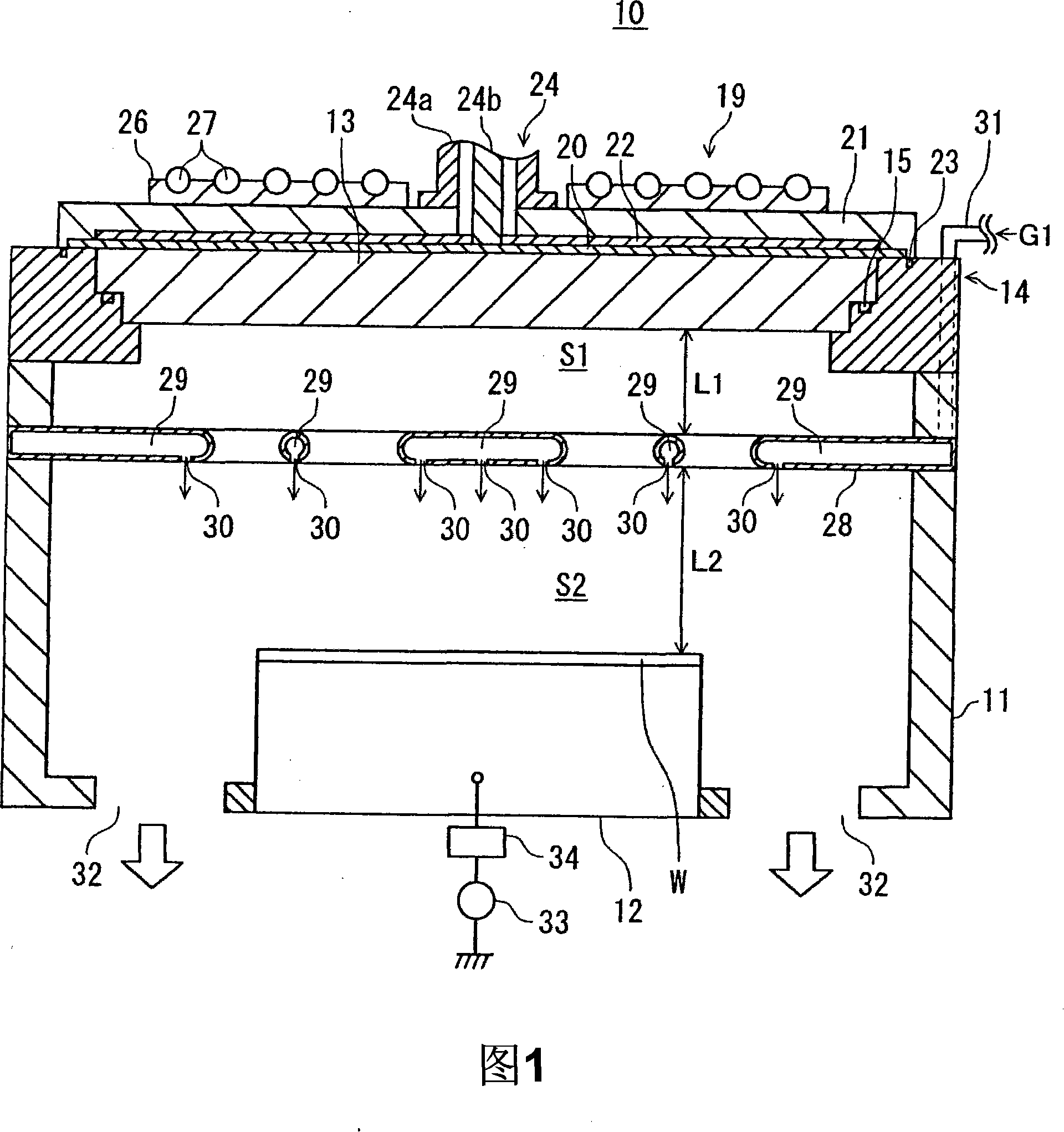
[0099] First, the wafer W shown in FIG. 4 is prepared, and the wafer W is loaded into the processing container 11 of the substrate processing apparatus 10, and HBr gas, O 2 gas and Ar gas, set the pressure of processing spaces S1 and S2 to 4.0Pa, supply 2.45GHz microwave to radial line slot antenna 19, and supply 400KHz high-frequency power to susceptor 12, and then pass through the opening The portion of the polysilicon film 37 exposed at 40 is etched to such an extent that only a small portion remains on the gate oxide film 36 . Then, HBr gas and He gas are supplied to the processing space S2, the pressure of the processing spaces S1 and S2 is set to 66.7 Pa, and the remaining polysilicon film is etched by plasma generated from the HBr gas or the like. At this time, it was confirmed that the residual polysilicon film was completely removed, and the gate oxide film 36 was hardly etched.
[0100] Next, the wafer W is carried into the processing container of the wet etching de...
Embodiment 2
[0108] First, under the same conditions as in Example 1, the portion of polysilicon film 37 exposed through opening 40 is etched to such an extent that only a little portion remains on gate oxide film 36 . Furthermore, the remaining polysilicon film was etched under the same conditions as in Example 1 except that the pressure in the processing spaces S1 and S2 was set to 33.3 Pa.
[0109] Then, the gate oxide film 36 exposed due to the complete removal of the residual polysilicon film is removed, and then the antireflection film 38 and the resist film 39 are removed. Afterwards, observing the gate of the wafer W, it can be confirmed that although the silicon substrate 35 slightly produces a recess, the depth of the recess is a depth limit that does not affect the doping of ions into the silicon substrate 35 (see FIG. 7(A)). In addition, it was also confirmed that the shape of the gate oxide film 36 was not expanded at the bottom of the gate.
Embodiment 3
[0111] First, under the same conditions as in Example 1, the portion of polysilicon film 37 exposed through opening 40 is etched to such an extent that only a little portion remains on gate oxide film 36 . Further, under the same conditions as in Example 1 except that the pressure of the processing spaces S1 and S2 was set to 93.3 Pa (700 mTorr), the remaining polysilicon film was etched.
[0112] Then, the gate oxide film 36 exposed due to the complete removal of the residual polysilicon film is removed, and then the antireflection film 38 and the resist film 39 are removed. Afterwards, the gate of the wafer W was observed, and it was confirmed that although no recess was formed on the silicon substrate 35, the shape of the gate oxide film 36 in the gate became a lower spread. The boundary of the lower part of the influence of doping ions into the silicon substrate 35 ( FIG. 7(B) ).
[0113] In Example 3, the pressure of the processing spaces S1 and S2 was set to 93.3 Pa dur...
PUM
 Abstract
Description
Claims
Application Information