Manufacturing method for semiconductor device and metal oxide semiconductor field effect transistor

A technology of field-effect transistors and oxide semiconductors, applied in semiconductor/solid-state device manufacturing, electrical components, circuits, etc., can solve problems such as leakage and interference of parasitic transistors, passivation of sharp edges and corners, etc.

Active Publication Date: 2008-04-02
MICROSOFT TECH LICENSING LLC
View PDF0 Cites 4 Cited by
  • Summary
  • Abstract
  • Description
  • Claims
  • Application Information

AI Technical Summary

Problems solved by technology

However, since this is an incidental side effect of the process of forming and subsequently removing the sacrificial dielectric layer 205, the sharp corner structures of the substrate 101 cannot be sufficiently passivated to overcome the possible Problems such as leakage and interference in parasitic transistors

Method used


Image

  • Manufacturing method for semiconductor device and metal oxide semiconductor field effect transistor
  • Manufacturing method for semiconductor device and metal oxide semiconductor field effect transistor
  • Manufacturing method for semiconductor device and metal oxide semiconductor field effect transistor

Examples


Embodiment Construction

[0039] The manner in which the various embodiments are made and used are described below. However, it should be noted that the various applicable inventive concepts provided by the present invention can be implemented according to various changes in the specific context, and the specific embodiments discussed here are only used to illustrate the specific use and manufacture of the present invention. method of invention, not intended to limit the scope of the invention.

[0040] The manufacturing process of the preferred embodiment of the present invention is described below through various drawings and examples. In addition, the same symbols represent the same or similar elements in various different embodiments and drawings of the present invention.

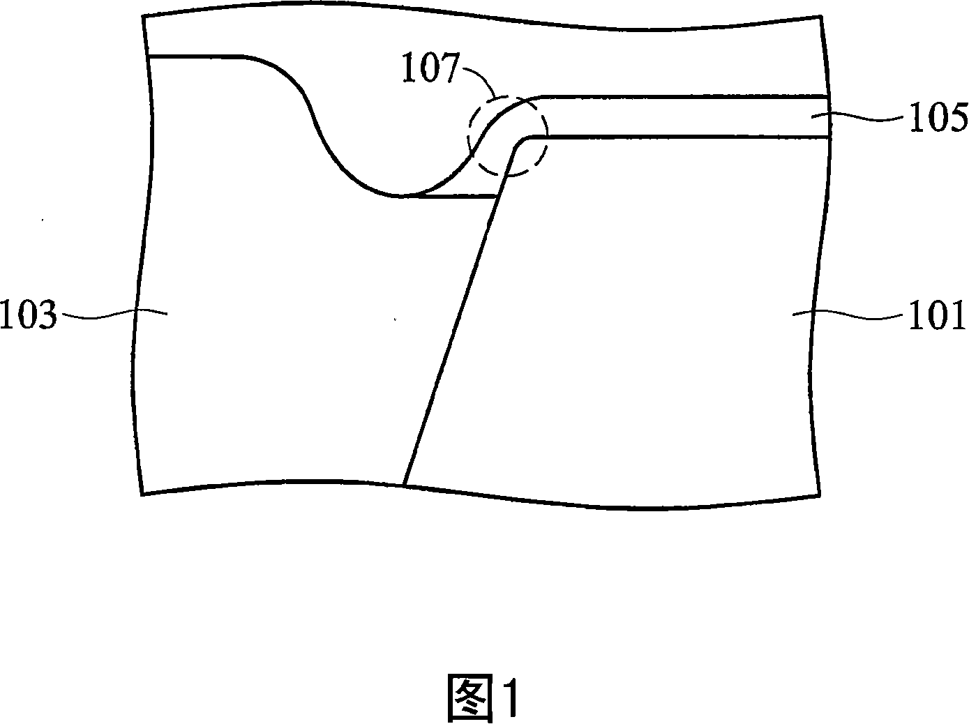
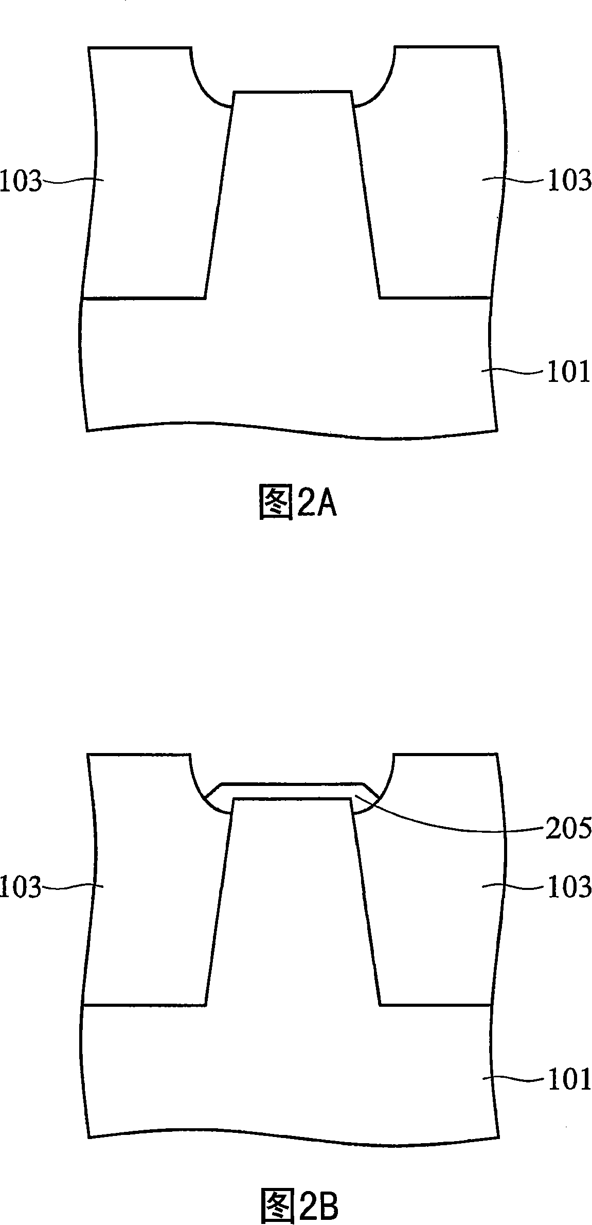
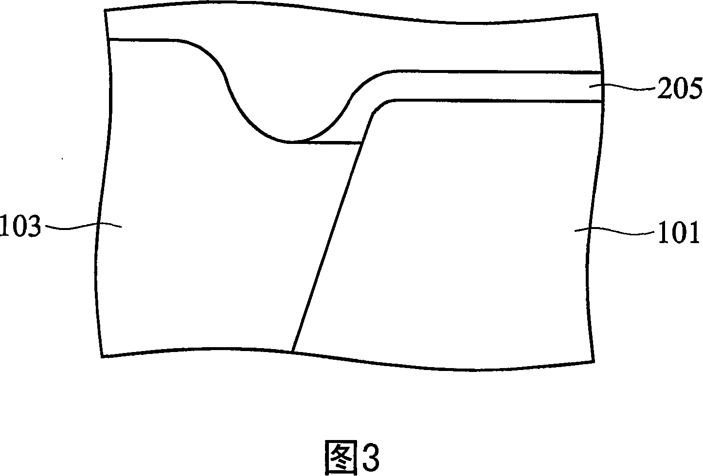
[0041] FIG. 4 shows a substrate 401 in which an isolation region 403 is formed. The substrate 401 may include doped or undoped silicon material, or an active layer of a silicon on insulator (SOI) substrate. A silicon-on-insul...


PUM


Abstract

The invention provides a semiconductor device and a fabricating method thereof, comprising following steps: A, providing a substrate including a separating zone formed therein; B, forming a dielectric layer on the the substrate and partial separating zone, wherein the dielectric layer has a first thickness; C, removing the dielectric layer; and D, repeating B to C twice or more. The invention makes the dielectric layer in the prospective region of the substrate have a larger thickness so as to reduce or eliminate the problems correlative to a parasitic transistor, break interference and leakage path.

Description

technical field [0001] The present invention relates to a method of manufacturing a semiconductor device, in particular to a method of manufacturing a metal oxide semiconductor field effect transistor. Background technique [0002] At present, the industry continues to try to reduce the size of semiconductor devices on silicon substrates. However, with the miniaturization of the size of semiconductor devices, many problems that do not have a significant impact on larger-sized devices have a critical impact on the operation of the devices after the miniaturization. Such a problem exists among thin dielectric layers formed on the semiconductor substrate adjacent to the isolation regions. [0003] FIG. 1 shows the above-mentioned problem, which occurs when the substrate 101 , the isolation region 103 and the gate dielectric layer 105 exist simultaneously. As mentioned above, the edge of the silicon substrate 101 adjacent to the isolation region 103 (usually a shallow trench i...

Claims


Application Information

Patent Timeline
Patent Type & Authority Applications(China)
IPC IPC(8): H01L21/762H01L21/31H01L21/82H01L21/336
Inventor 王驭熊朱文定陈恒毅金显维
Owner MICROSOFT TECH LICENSING LLC
Why Eureka
Try Eureka