Semi-conductor memory device and manufacturing method thereof

A technology for storage devices and manufacturing methods, which is applied in semiconductor/solid-state device manufacturing, semiconductor devices, electric solid-state devices, etc., can solve problems such as the inability to use high-density memory, excessive flash memory unit area, etc., to avoid excessive unit area Large, avoiding the effects of low storage efficiency and reduced unit area

Inactive Publication Date: 2008-04-02
SEMICON MFG INT (SHANGHAI) CORP
View PDF1 Cites 18 Cited by
  • Summary
  • Abstract
  • Description
  • Claims
  • Application Information

AI Technical Summary

Problems solved by technology

[0006] The problem solved by the present invention is that the flash memory cell area is too large and cannot be used in high-density memory

Method used


Image

  • Semi-conductor memory device and manufacturing method thereof
  • Semi-conductor memory device and manufacturing method thereof
  • Semi-conductor memory device and manufacturing method thereof

Examples


Embodiment Construction

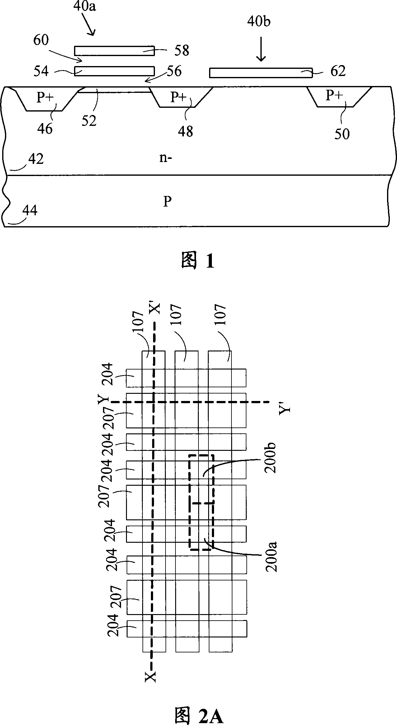
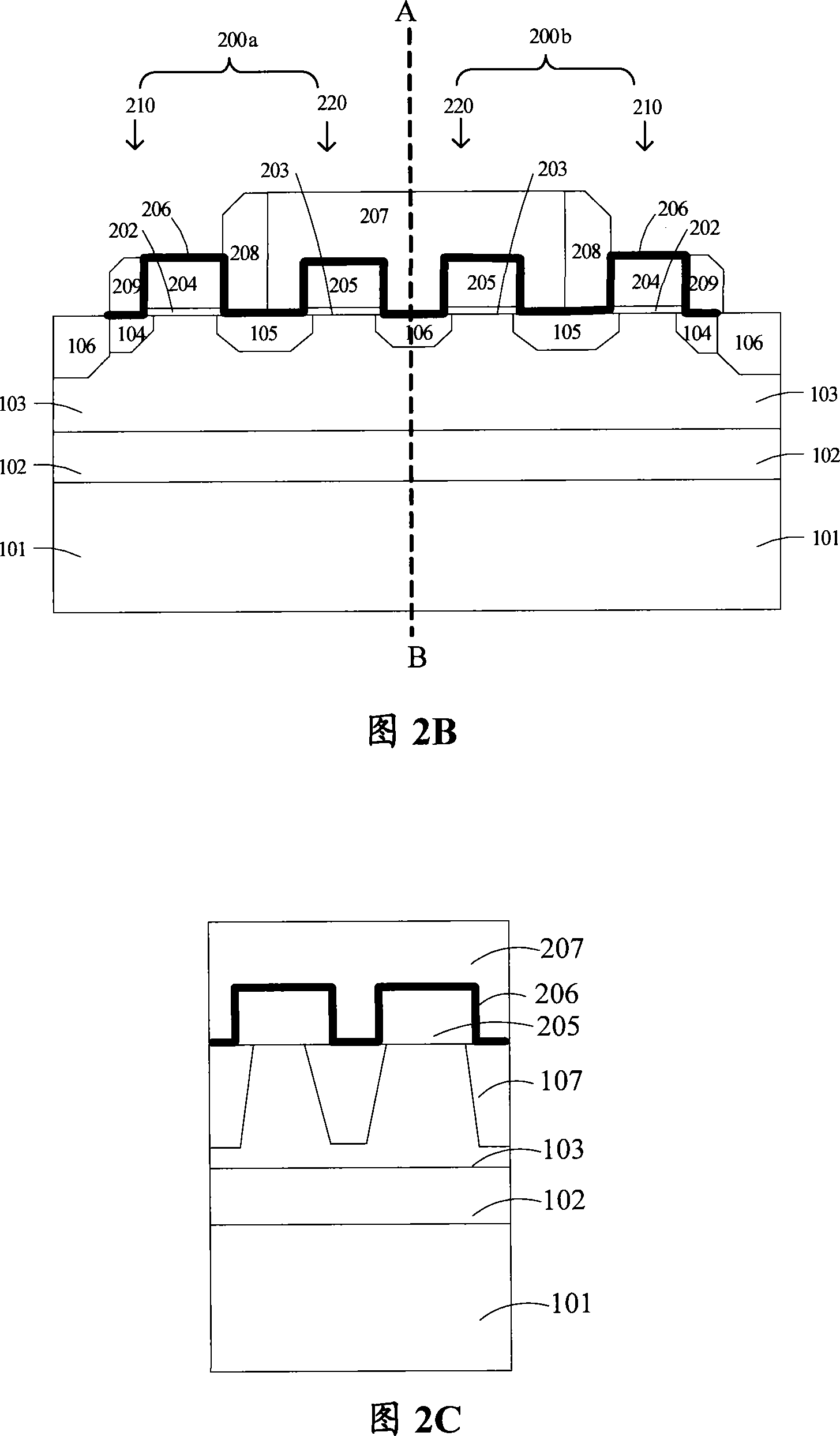
[0045]A layout diagram of an embodiment of the semiconductor memory device of the present invention is shown in FIG. 2A. As shown in FIG. 2A, at least one memory cell pair is distributed, and each memory cell pair includes a memory cell 200a and a memory cell 200b. The memory cell pairs are arranged serially in XX', that is, the bit line direction, and each memory cell pair is distributed with the selection gate 204 of the memory cell 200a along the bit line direction, sharing the control gate 207 and the selection gate 204 of the memory cell 200b, Wherein the selection gates 204 of the memory cells 200a, 200b are symmetrical about the common control gate 207; the memory cell pairs are arranged in parallel in the YY' direction, that is, the word line direction, and the select gates 204 and the common control gate 207 of the adjacent memory cell pairs share a common Line-aligned distribution, parallel to the Y-Y' axis. Adjacent memory cell pairs in the X-X' and Y-Y' directions ...


PUM


Abstract

The invention provides a semiconductor memory device, comprising at least one memory unit pair wherein, each memory unit comprises a floating gate transistor and a selection transistor; the two floating gate transistor of the memory unit pair comprise a common source, two drains and two floating gates, wherein, the two floating gates have a common control gate; with voltage applied on the control gate, an conducting channel formed inside a semiconductor substrate connects the common source and the corresponding drains electrically. Accordingly, the invention provides an arrangement of and a method for manufacturing the semiconductor memory device, wherein, the common control gate controls the floating gates at the same time, which reduces the unit area and improves the memory density; meanwhile, common control gate is in complete contact with an interlayer insulated layer, which improves the floating gate coupling capacitor as well as the memory efficiency.

Description

technical field [0001] The invention relates to a semiconductor memory, in particular to a non-volatile semiconductor memory and a manufacturing method thereof. Background technique [0002] There are several forms of non-volatile memory currently available, including electrically programmable read-only memory (EPROM), electrically erasable programmable read-only memory (EEPROM), and flash memory. Flash memory (flash memory) has the characteristics of non-volatility for storing data, low power consumption, electrical rewritability, and low cost. Therefore, in recent years, as a small and portable information processing tool, flash memory has been widely used in Devices such as memory cards, personal digital assistants (PDA's, Personal Digital Assistant), cellular phones, mobile information terminals, and MP3 players are used for large-capacity data storage. In order to make its market larger, it is important to make the area of ​​the memory cell smaller, thereby reducing th...

Claims


Application Information

Patent Timeline
Patent Type & Authority Applications(China)
IPC IPC(8): H01L27/115H01L21/8247
Inventor 金钟雨肖德元
Owner SEMICON MFG INT (SHANGHAI) CORP
Why Eureka
Try Eureka