Solar cell manufacturing method, solar cell, and semiconductor device manufacturing method
A technology of solar cells and manufacturing methods, applied in semiconductor/solid-state device manufacturing, semiconductor devices, final product manufacturing, etc., can solve problems such as inconvenience and low conversion efficiency
- Summary
- Abstract
- Description
- Claims
- Application Information
AI Technical Summary
Problems solved by technology
Method used
Image

Examples
Embodiment 1
[0153] Embodiment 1, comparative example 1
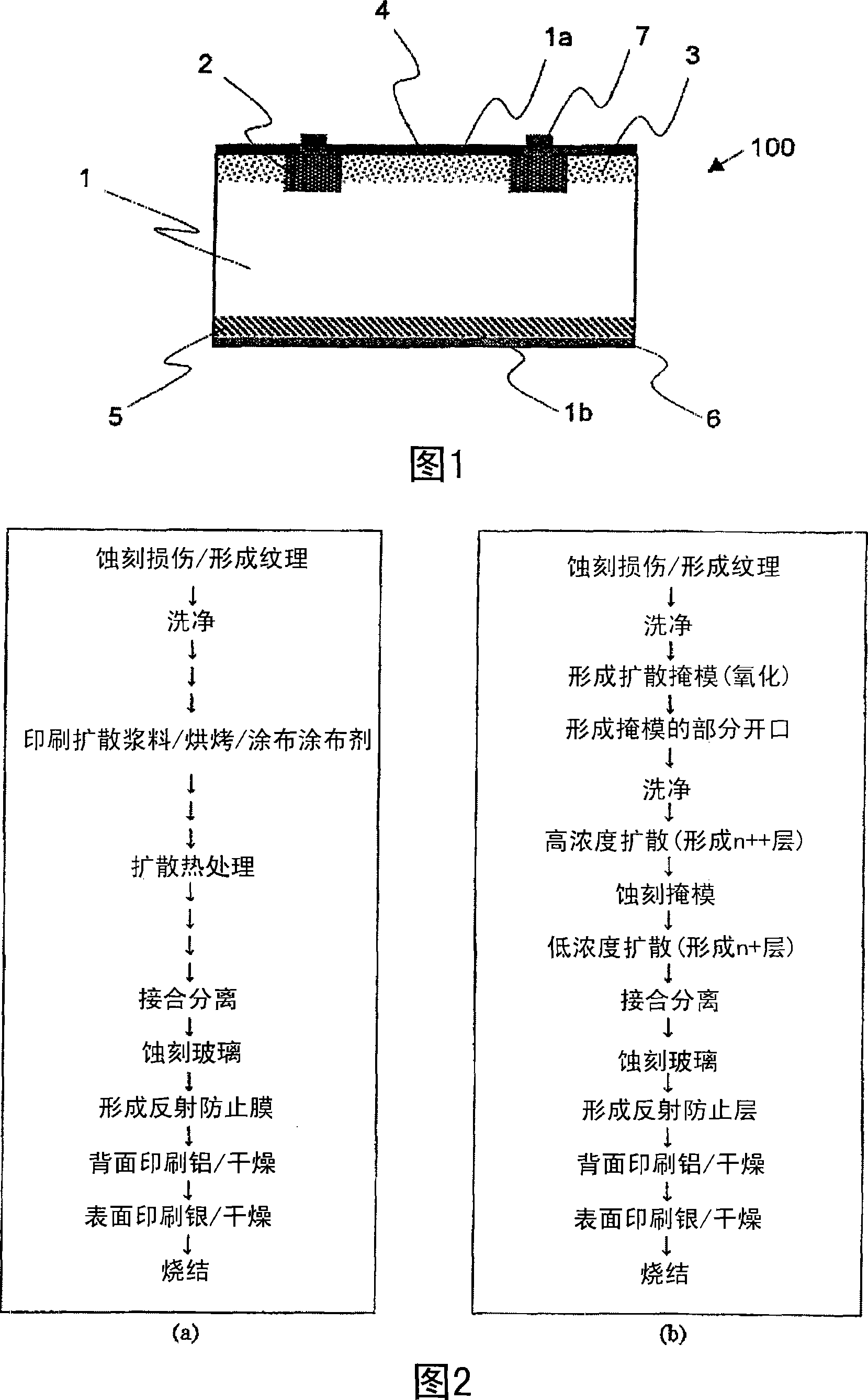
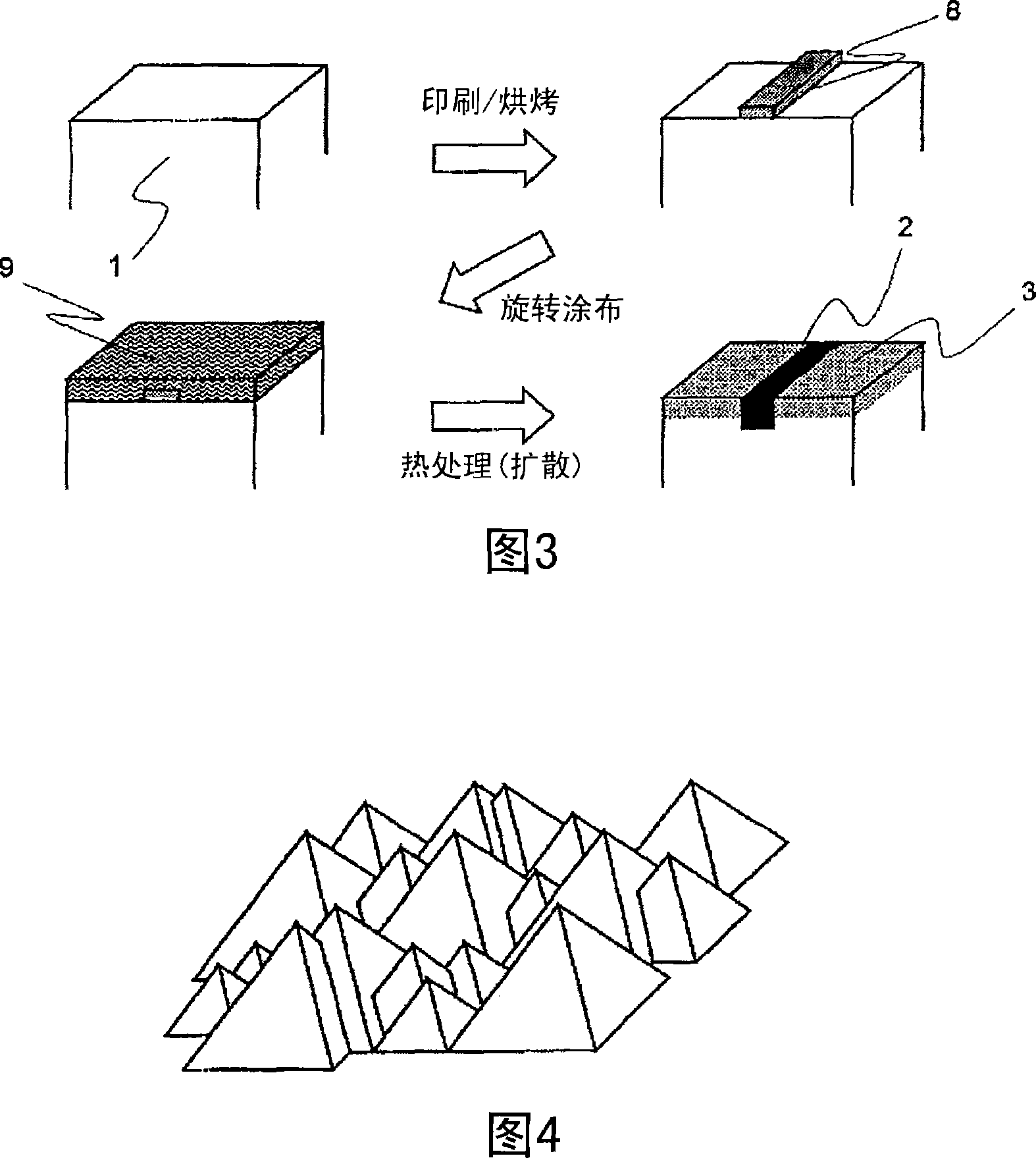
[0154] Example 1, according to the process of Figure 2(a), using the CZ method, the crystal plane orientation is (100), 15cm square, 250μm thick, and the resistivity after slicing is 2Ω.cm (the dopant concentration is 7.2× 10 15 cm -3 ), gallium-doped single-crystal silicon substrate whose first conductivity type is P-type, is immersed in 40% by weight sodium hydroxide aqueous solution, and the damaged layer is etched away. Second, the substrate was wet-etched by immersing the substrate in an aqueous solution in which isopropanol was added to 3% by weight of sodium hydroxide to form random textures on the surface.
[0155] Then, after the substrate is cleaned, the diffusion paste containing phosphoric acid and silica gel is printed and coated on the light-receiving surface of the substrate with a screen printing machine. The printed pattern at this time was a linear pattern with a pitch of 2 mm and a width of 150 μm. The printed...
Embodiment 2
[0165] Embodiment 2 A solar cell is manufactured by various two-stage emitter manufacturing methods of the present invention. Table 2 shows the sheet resistances of the high-concentration layer and the low-concentration layer formed at this time. The characteristics of those solar cells are combined in Table 3.
[0166] As shown in Table 2, in order to form two kinds of concentration diffusion layers in the same plane by the coating diffusion method, this embodiment utilizes the dopant content contained in the coating agent, coating thickness, glass content (silicon compound content ), elements, etc. In particular, changes in viscosity or grooves were used for changes in coating thickness.
[0167] The method for making the two-stage emitter is briefly described below. In addition, a series of processes from formation of texture, diffusion to formation of electrodes are the same as those in Embodiment 1.
[0168] First, for samples A, C, D, and E, by changing the items sho...
Embodiment 3
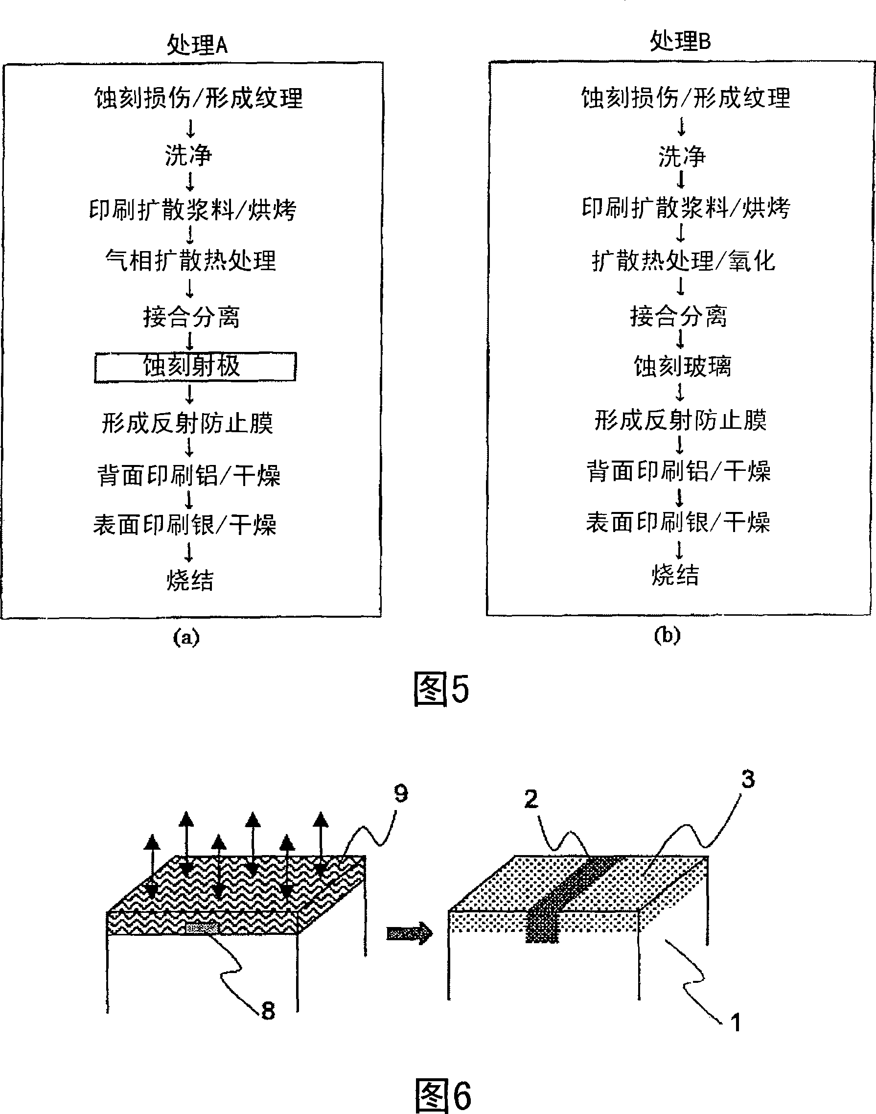
[0176] Solar cells were manufactured according to the processes of treatments A and B shown in FIG. 5 . Except for the etch-back and surface oxidation of the surface of the diffusion layer, other manufacturing conditions are the same as in Example 1. At this time, etch back is performed after heat treatment, that is, the substrate is immersed in an ammonia / hydrogen peroxide aqueous solution to etch the surface by several nanometers. On the other hand, the surface oxidation is a continuous heat treatment, and the substrate is kept in a heat treatment furnace for 10 minutes without cooling down, but only by flowing dry oxygen. Various characteristics of the solar cell obtained according to this example are shown in Table 4. Various characteristics of the solar cell of Example 1 are also shown in Table 4 for comparison. Spectral sensitivity characteristics (external quantum efficiency) are shown in FIG. 10 .
[0177] [Table 4]
[0178] open circuit voltage
(V...
PUM
| Property | Measurement | Unit |
|---|---|---|
| electrical resistivity | aaaaa | aaaaa |
| thickness | aaaaa | aaaaa |
| electrical resistivity | aaaaa | aaaaa |
Abstract
Description
Claims
Application Information
 - R&D
- Intellectual Property
- Life Sciences
- Materials
- Tech Scout
- Unparalleled Data Quality
- Higher Quality Content
- 60% Fewer Hallucinations
Browse by: Latest US Patents, China's latest patents, Technical Efficacy Thesaurus, Application Domain, Technology Topic, Popular Technical Reports.
© 2025 PatSnap. All rights reserved.Legal|Privacy policy|Modern Slavery Act Transparency Statement|Sitemap|About US| Contact US: help@patsnap.com