An outside cavity high-power semiconductor laser alternating array power

A semiconductor and laser technology, applied in the field of external cavity high-power semiconductor laser array light sources, can solve the problems of parallel coupling, difficult industrialization, and inconvenient semiconductor laser array assembly.

Inactive Publication Date: 2008-04-30
长春德信光电技术有限公司
View PDF1 Cites 8 Cited by
  • Summary
  • Abstract
  • Description
  • Claims
  • Application Information

AI Technical Summary

Problems solved by technology

In this scheme, a plano-concave lens is used. Due to the divergence of the plano-concave lens, the focused beams a and c cannot be coupled to the grating in parallel; On the focal point of the spherical reflector, to the stacking array of semiconductor lasers, in order to make the laser beam of each layer of the stacking array of semiconductor lasers converge on the focus of the spherical reflector through the double-convex spherical lens, as shown in Figure 6 (CN 1829015A) scheme, The diameter of the double-convex spherical lens needs to be larger than the size of the semiconductor laser stack, which is inconvenient to assemble with the semiconductor laser stack and difficult for industrialization

Method used


Image

  • An outside cavity high-power semiconductor laser alternating array power
  • An outside cavity high-power semiconductor laser alternating array power
  • An outside cavity high-power semiconductor laser alternating array power

Examples


Embodiment 1

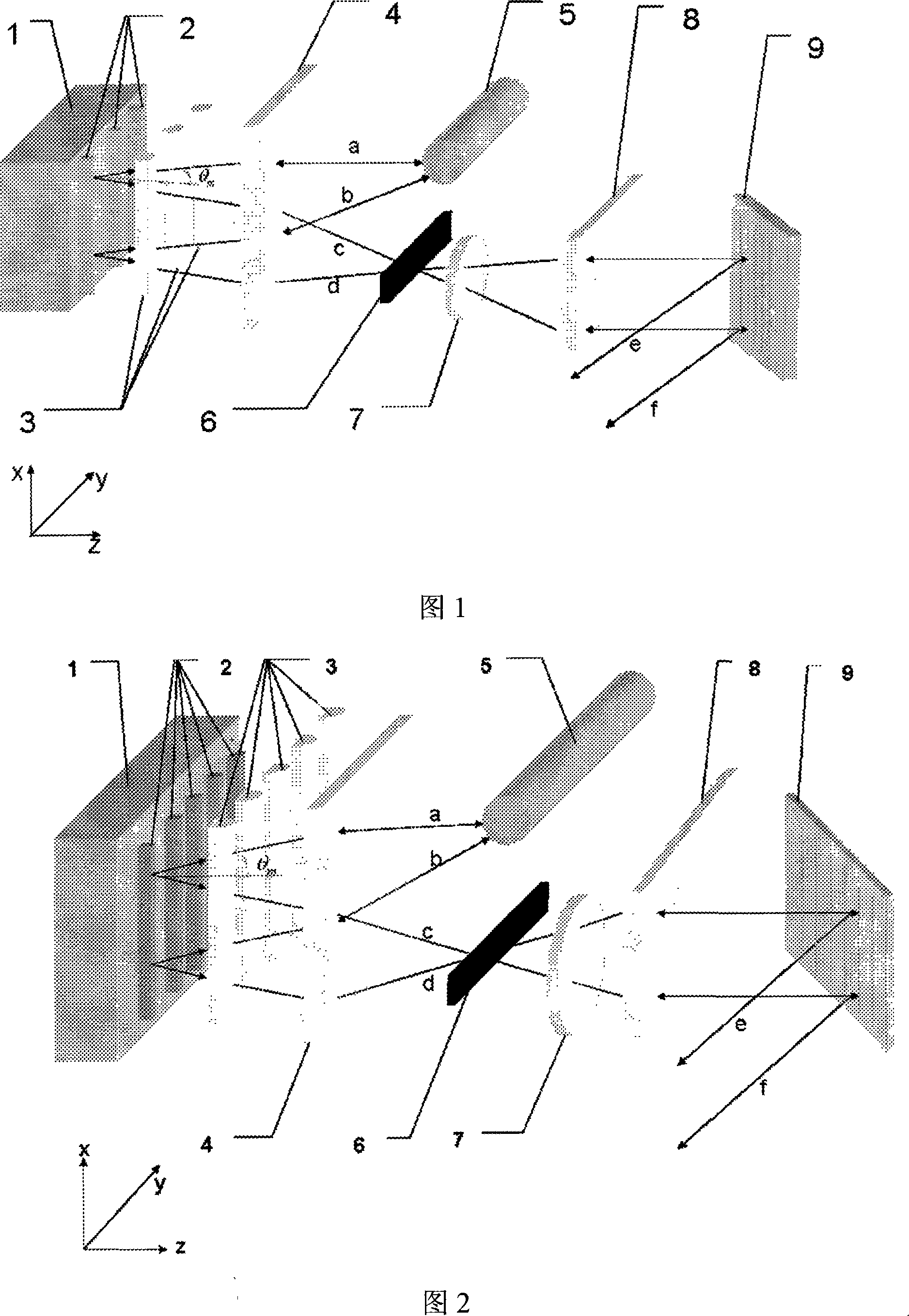
[0029] Referring to accompanying drawing 1, semiconductor laser stacked array 1 is formed by stacking 3 semiconductor laser arrays 2, layer spacing is 5mm, y direction length is 1.2cm, x direction length is 1.2cm, emission wavelength is 808nm, each semiconductor laser The fast axis direction (y direction in FIG. 1 ) of the line array 2 is provided with respective fast axis collimating mirrors 3 to collimate the fast axis. The fast-axis collimating mirror 3 is a microcylindrical lens. The lasers a, b, c, and d after the fast-axis collimation are approximately parallel light in the fast-axis direction, and the slow-axis direction (the x direction in FIG. 1 ) is divided into two paths. A path of light a and b propagating upward forms an upper far-field lobe; a path of light c and d propagating downward forms a lower far-field lobe. The angle between the upper optical path a, b and the lower optical path c, d and the optical axis (z direction in Figure 1) before entering the fast ...

Embodiment 2

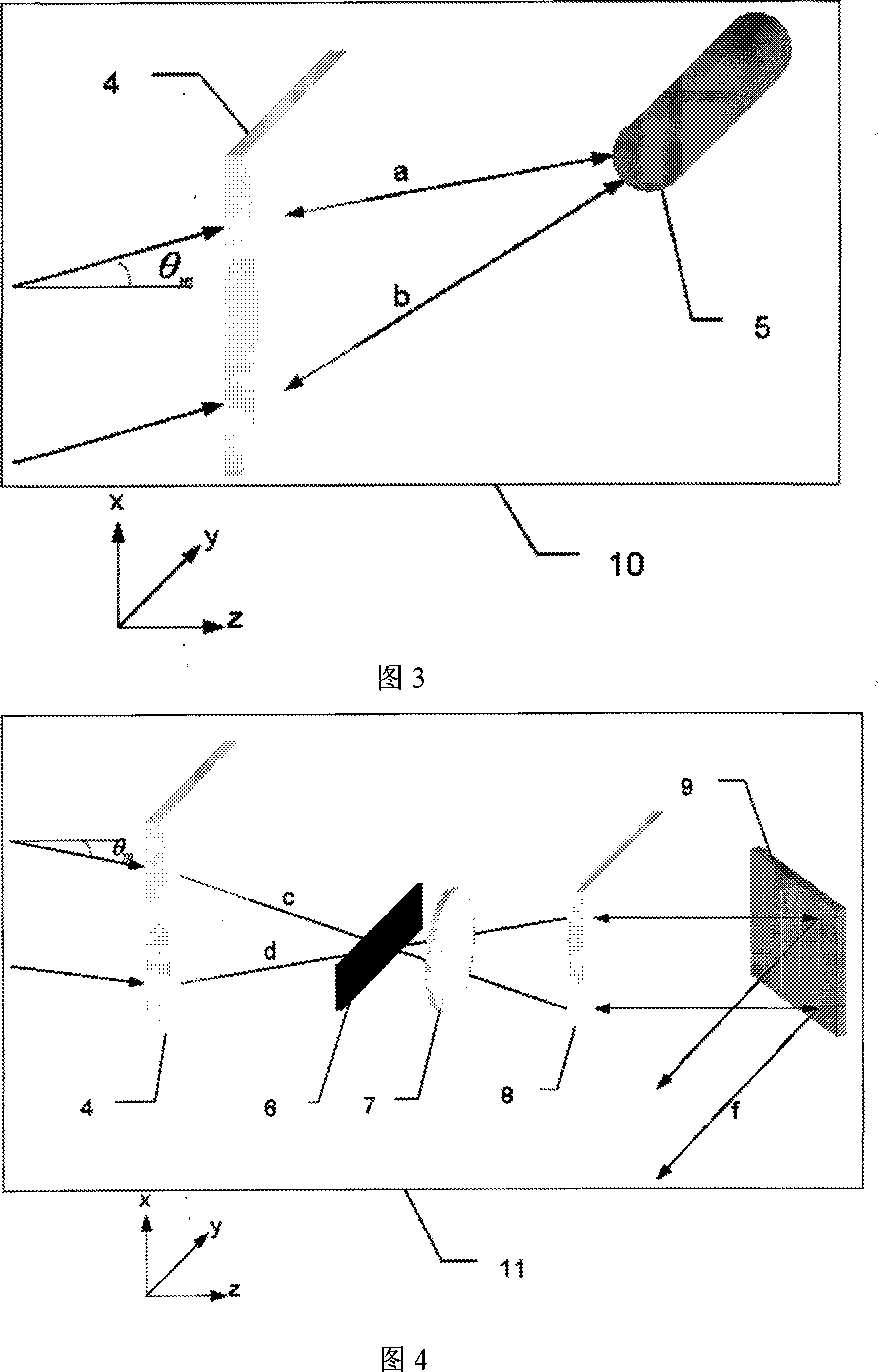
[0034] Referring to accompanying drawing 2, semiconductor laser stacked array 1 is formed by stacking 5 semiconductor laser arrays 2, layer spacing is 4mm, y direction length is 2.0cm, x direction length is 1.2cm, emission wavelength is 980nm, semiconductor laser array The fast axis direction of 2 (the y direction in FIG. 2 ) is provided with respective fast axis collimating mirrors 3 to collimate the fast axis. The fast-axis collimating mirror 3 is an aspheric lens. The lasers a, b, c, and d after the fast-axis collimation are approximately parallel light in the fast-axis direction, and the slow-axis direction (the x direction in FIG. 2 ) is divided into two paths. A path of light a and b propagating upward forms an upper far-field lobe; a path of light c and d propagating downward forms a lower far-field lobe. The angle between the upper optical path a, b and the lower optical path c, d and the optical axis (z direction in Figure 2) before entering the fast axis collimator i...


PUM

PropertyMeasurementUnit
lengthaaaaaaaaaa
lengthaaaaaaaaaa

Abstract

An array light source for a pericoel high-power semiconductor laser is provided, which utilizes a collimating mirror to conduct collimation to a fast axis, utilizes two convex-plane cylindrical mirrors to conduct collimation to a slow axis, the light of the collimated fast axis is divided into two roads for propagation, a cylindrical reflector and a raster are separately utilized to conduct feedback to the two roads of light, thereby realizing laser output of lightness and narrow line width of semiconductor laser array. The rectangular convex-plane cylindrical mirrors and the cylindrical reflector are relatively easy to be assembled with the semiconductor laser array. In addition, the laser output brightness can be adjusted through adjusting rectangular slit width, and the output laser power can be adjusted through rotating the half-wave plate.

Description

technical field [0001] The invention belongs to the field of high-power semiconductor lasers, and relates to an external-cavity high-power semiconductor laser array light source. Background technique [0002] Due to its compact structure, high efficiency and long life, high-power semiconductor laser arrays are widely used in many fields, such as material processing, laser marking, laser medical treatment, pumping solid-state lasers, spin exchange optical pumping (SEOP) and other fields . However, due to the large divergence angle and wide spectral bandwidth of semiconductor lasers, its application is greatly limited. [0003] The output beam quality of semiconductor laser can be improved by external cavity feedback. Most of the commonly designed external cavity semiconductor lasers are aimed at low-power single-tube semiconductor lasers [Opt.Lett.27, 1995 (2002)]. [0004] For the high-power, high-brightness, and narrow-linewidth laser output of semiconductor laser arrays...

Claims


Application Information

Patent Timeline
Patent Type & Authority Applications(China)
IPC IPC(8): H01S5/40H01S5/14G02F1/00
Inventor 邓鑫李王峙皓
Owner 长春德信光电技术有限公司
Why Eureka
Try Eureka