
Method of inspecting defect for electroluminescence display apparatus, repairing method and manufacturing method

An electroluminescence display and manufacturing method technology, applied in electroluminescence light sources, electric light sources, measuring devices, etc., can solve problems such as inspection methods that have not yet been established, and achieve the effects of easy automatic defect determination and improved correction efficiency.

Inactive Publication Date: 2008-05-07
SANYO ELECTRIC CO LTD +1
View PDF2 Cites 20 Cited by
  • Summary
  • Abstract
  • Description
  • Claims
  • Application Information

AI Technical Summary

Problems solved by technology

However, an effective inspection method corresponding to the cause has not yet been established

Method used


Image

  • Method of inspecting defect for electroluminescence display apparatus, repairing method and manufacturing method
  • Method of inspecting defect for electroluminescence display apparatus, repairing method and manufacturing method
  • Method of inspecting defect for electroluminescence display apparatus, repairing method and manufacturing method

Examples


Embodiment Construction

[0045] Hereinafter, the best mode of carrying out this invention (hereinafter referred to as "embodiment") will be described with reference to the drawings.

[0046] [check principle]

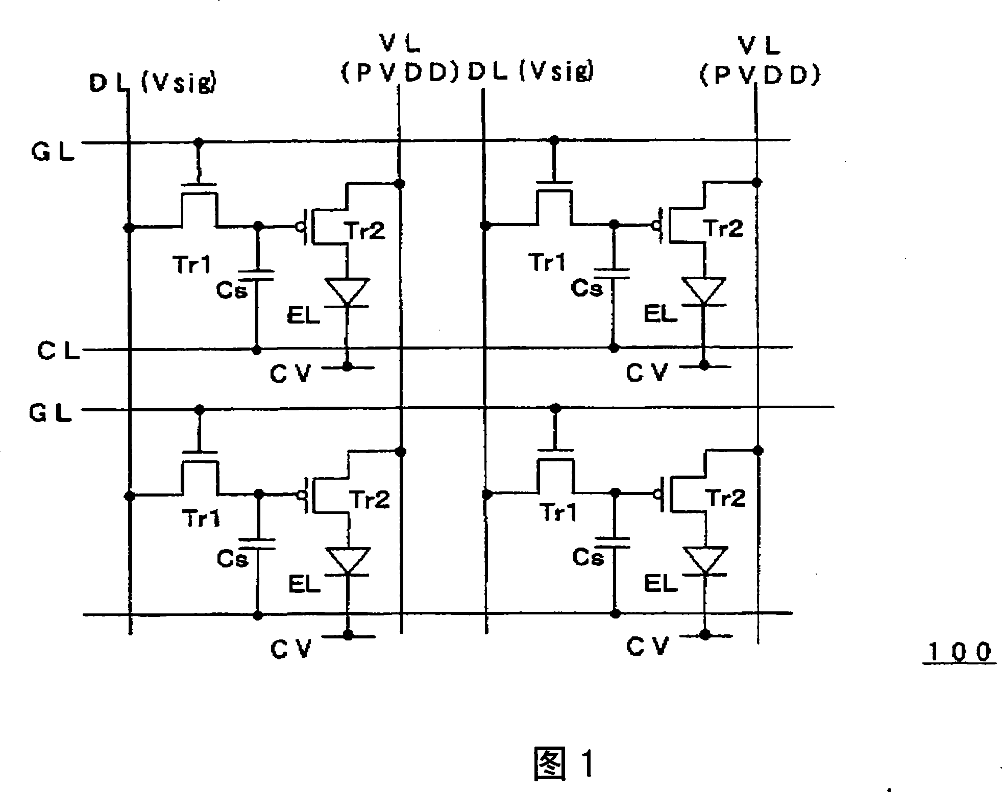
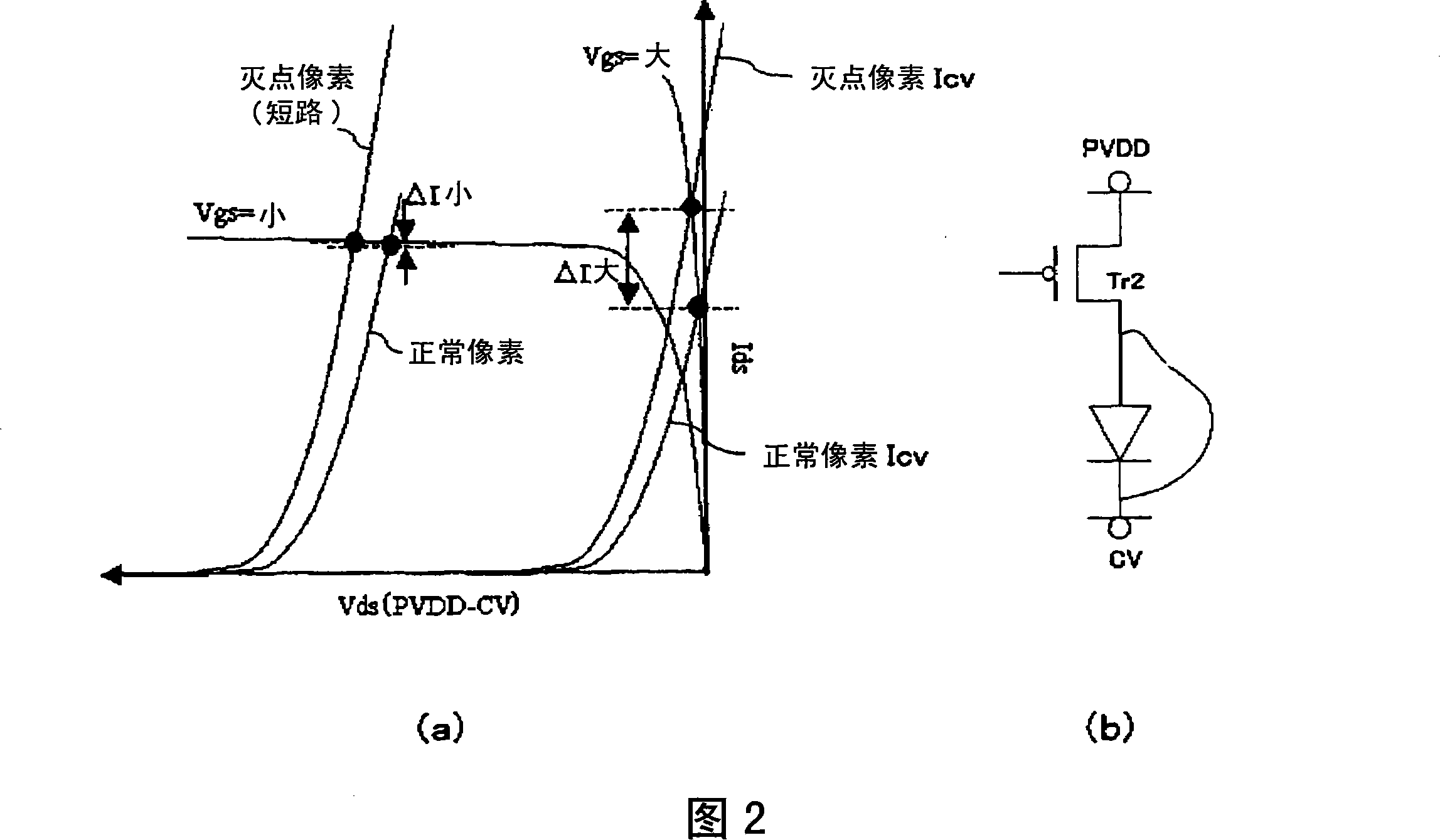
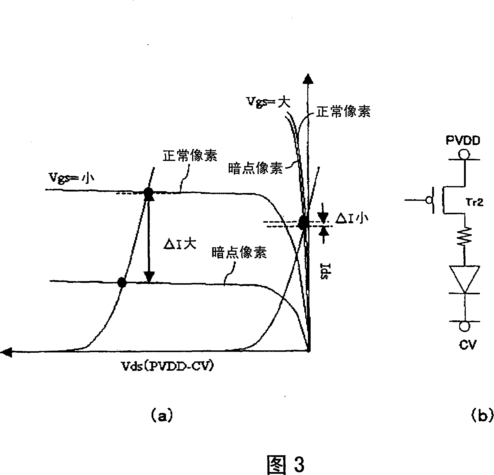
[0047] In the present embodiment, the display device is specifically an active matrix organic EL display device, and a display unit including a plurality of pixels is formed on the EL panel 100 . FIG. 1 is a diagram showing an equivalent circuit configuration of an active matrix display device in this embodiment, and FIGS. 2 and 3 show the principle of defect inspection for each pixel of the EL display device used in this embodiment. In the display portion of the EL panel 100, a plurality of pixels are arranged in a matrix, and in the horizontal scanning direction (row direction) of the matrix, selection lines GL for sequentially outputting selection signals are formed, and in the vertical scanning direction (column direction), A data line DL for outputting a data signal and a power line VL fo...


PUM


Abstract

The present invention provides a defect detecting method for electroluminescent display device. A dark spot defect caused by short-circuiting in an electroluminescence element is detected based on an emission brightness or a current flowing through the electroluminescence element when an element driving transistor which controls a drive current supplied to the electroluminescence element is operated in its linear operating region and the electroluminescence element is set to an emission level. Prior to the dark spot defect inspection, the dark spot defect is screened by applying a reverse bias voltage between an anode and a cathode of the electroluminescence element. With this process, disappearance of the dark spot defect at a later time resulting in an impossibility of laser repairing or the like is prevented, and inspection and repairing efficiencies are improved. A dim spot defect caused by a characteristic variation of the element driving transistor is detected based on a current flowing through the electroluminescence element or an emission brightness when the element driving transistor is operated in its saturation operating region and the electroluminescence element is set to an emission level.

Description

technical field [0001] The present invention relates to inspection of defects caused by electroluminescent elements of a display device having electroluminescent elements in each pixel, or defects caused by transistors driving the electroluminescent elements. Background technique [0002] An EL display device using an electroluminescent element (hereinafter referred to as an EL element) as a self-luminous element as a display element of each pixel is expected as a next-generation flat display device, and research and development are being conducted. [0003] Such an EL display device is shipped as a product after several inspections are performed after the EL panel is formed on a substrate such as glass or plastic, and an EL panel such as a thin-film transistor (TFT) for driving the EL element for each pixel. . In current EL display devices, improvement in yield is very important, and improvement in manufacturing processes of EL elements and TFTs, improvement in materials, ...

Claims


Application Information

Patent Timeline
Patent Type & Authority Applications(China)
IPC IPC(8): G09G3/00G09G3/30G01R31/00G01R31/02G01R31/26G01M11/02
CPCH05B33/10
Inventor 小川隆司
Owner SANYO ELECTRIC CO LTD
Learn More