Silicon Carbide Rectifier

a silicon carbide rectifier and silicon carbide technology, applied in the direction of basic electric elements, electrical equipment, semiconductor devices, etc., can solve the problems of negative temperature coefficient of forward voltage drop, thermal runaway, negative temperature coefficient of conventional silicon carbide pin rectifiers, etc., to reduce reverse recovery charge, reduce carrier density, and reduce current value

Active Publication Date: 2013-09-19
U S A AS RPRESENTED BY THE SEC OF THE NAVY THE
View PDF3 Cites 5 Cited by
  • Summary
  • Abstract
  • Description
  • Claims
  • Application Information

AI Technical Summary

Benefits of technology

[0004]Improved PiN diodes or rectifiers are provided that have lower current value for the crossover point. The improved PiN diodes can have lower carrier density in the drift layer for reduced reverse recovery charge and reduced reverse recovery peak currents. The improved PiN diodes can also have temperature compensated operation. Improved PiN diodes or rectifiers are provided having a lower current value for the crossover point at which the overall temperature coefficient of forward voltage drop shifts from a negative temperature coefficient to a positive temperature coefficient by which the current density advantages of conventional SiC PiN diodes may be achieved while mitigating or avoiding thermal runaway conditions. An n type drift layer is provided over an n type silicon carbide or gallium nitride substrate in certain embodiments, where the drift layer has a lower dopant concentration than that of the substrate. A p type anode layer is provided on the drift layer, and one or more p type anode contact structures are disposed on the upper surface of the p type anode layer, having higher dopant concentration than the p type anode layer. The individual p type anode contact structures are laterally spaced from one another and define a total upper surface area that is less than the surface area of the upper surface of the p type anode layer. Metal electrical contacts are formed along the upper surfaces of the p type anode contact structures, and an anode metal layer is connected to the upper surfaces of the metal electrical contacts. The current crowding in the anode layer debiases the anode over a portion of the anode layer. This reduction in the p type anode contact area relative to the anode surface area provides a spreading resistance, where the anode debias increases with current and thereby lowers the current value of the crossover point and results in reduced carrier injection from the anode into the drift layer and thus reduced carrier density in the drift layer and reduced reverse recovery charge. The crossover point is the current value at which the temperature coefficient of the device shifts from a negative temperature coefficient of forward voltage to a positive temperature coefficient of forward voltage. The crossover point is also known as the temperature independent point and is also known as the zero temperature coefficient value. This, in turn, mitigates or overcomes the disadvantages of conventional silicon carbide PiN diodes while providing higher current density operation than similarly-sized silicon carbide Schottky rectifiers.
[0005]In certain embodiments, the acceptor doping level in the p type anode layer is significantly reduced and / or the p type anode layer is made very thin, thereby increasing the layer resistivity. This, in turn, causes the crossover point to occur at lower current levels. Moreover, certain embodiments provide a positive temperature coefficient for the metal-semiconductor electrical contact resistance of the p type anode contact structure / metal electrical contact interface, thereby lowering the current value of the silicon carbide PiN power rectifier structure at which the device has a positive temperature coefficient.

Problems solved by technology

However, conventional silicon carbide PiN rectifiers suffer from negative temperature coefficient of forward voltage drop due to the relatively deep acceptor dopant energy level in the p type emitter of the PiN structure.
The increased current level, in turn, raises the junction temperature further, leading to thermal runaway, which is particularly problematic when multiple SiC PiN rectifiers are connected in parallel.
Consequently, conventional silicon carbide PiN rectifiers suffer from negative temperature coefficient problems.

Method used


Image

  • Silicon Carbide Rectifier
  • Silicon Carbide Rectifier
  • Silicon Carbide Rectifier

Examples


Embodiment Construction

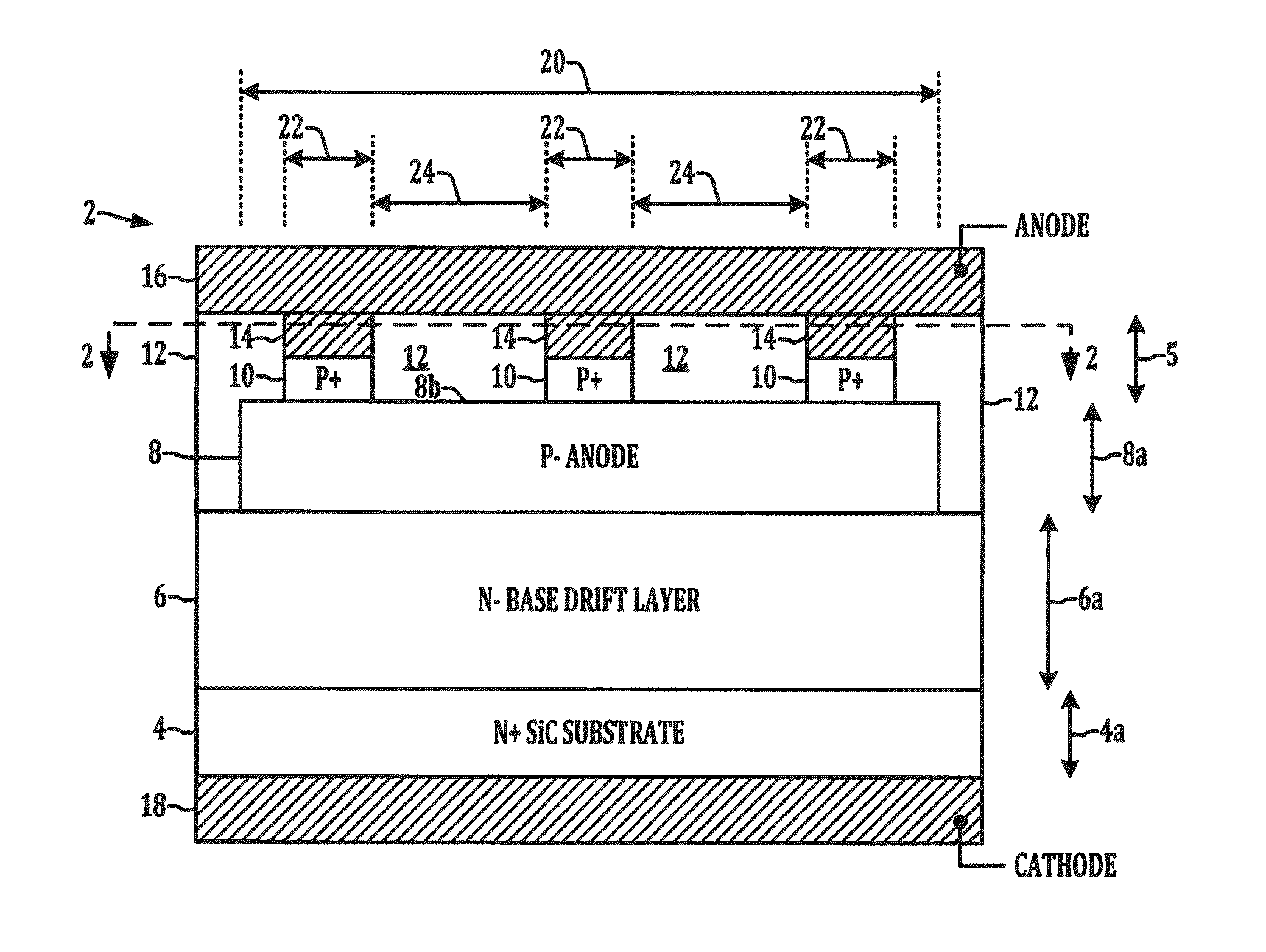
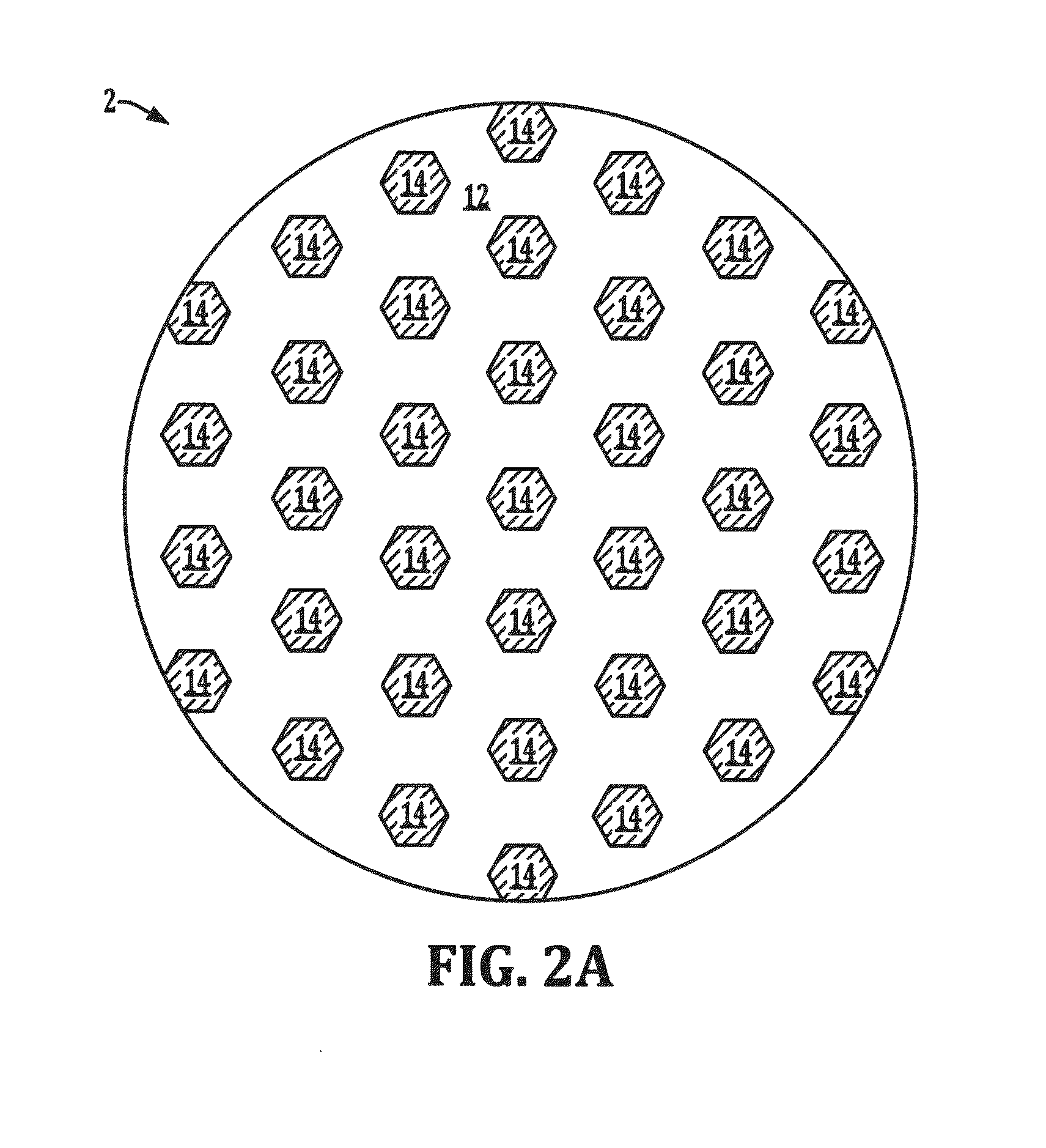
[0018]One or more embodiments or implementations are hereinafter described in conjunction with the drawings, where like reference numerals refer to like elements throughout, and where the various features are not necessarily drawn to scale. FIGS. 1 and 2A-2D illustrate certain embodiments of a low crossover point silicon carbide PiN diode or power rectifier 2 with limited anode contact area in accordance with one or more aspects of the present disclosure, and FIG. 3 shows an exemplary process 50 for fabricating the rectifier 2. Several embodiments of improved SiC PiN diodes or rectifiers are described herein, having reduced or lowered current value for the crossover point between positive and negative temperature coefficient of forward voltage. The improved SiC PiN diodes in certain implementations may advantageously have lower carrier density in the drift layer for reduced reverse recovery charge and reduced reverse recovery peak currents.

[0019]As best seen in FIG. 1, the rectifier...


PUM

PropertyMeasurementUnit
thicknessaaaaaaaaaa
thicknessaaaaaaaaaa
thicknessaaaaaaaaaa

Abstract

Silicon carbide PiN diodes are presented with reduced temperature coefficient crossover points by limited p type contact area to limit hole injection in the n type drift layer in order to provide a lower current at which the diode shifts from negative temperature coefficient to a positive temperature coefficient of forward voltage for mitigating thermal runaway.

Description

REFERENCE TO RELATED APPLICATION[0001]This application claims priority to and the benefit of U.S. Provisional Patent Application Ser. No. 61 / 532,212, filed Sep. 8, 2011, and entitled “Temperature Compensated SiC Power Rectifier”, the entirety of which is hereby incorporated by reference.BACKGROUND[0002]Power rectifiers are used in a variety of applications, such as passive rectifier circuits to rectify AC supply power, and as anti-parallel diodes across an insulated gate bipolar transistor (IGBT), where multiple power rectifiers are often connected in parallel with one another to achieve a desired current rating. PiN diodes are often used in high switching speed applications, and include a lightly doped near-intrinsic region situated between more highly doped P and N regions to facilitate high level injection of carriers from the P and N regions. For high power applications, Silicon Carbide (SiC) PiN rectifiers are sometimes used, where silicon carbide advantageously provides higher...

Claims


Application Information

Patent Timeline
Patent Type & Authority Applications(United States)
IPC IPC(8): H01L29/16H01L21/02H01L29/20
CPCH01L29/6606H01L29/66136H01L29/66143H01L29/8613H01L29/872H01L29/417H01L29/0692H01L29/1608H01L29/2003H01L21/02365H01L29/0657
Inventor HOBART, KARL D.KUB, FRANCIS J.ANCONA, MARIOIMHOFF, EUGENE A.
Owner U S A AS RPRESENTED BY THE SEC OF THE NAVY THE
Why Eureka
Try Eureka