
Layout interconnections verifying apparatus and method for verifying layout interconnections

Inactive Publication Date: 2005-09-22
RENESAS ELECTRONICS CORP
View PDF6 Cites 0 Cited by
  • Summary
  • Abstract
  • Description
  • Claims
  • Application Information

AI Technical Summary

Benefits of technology

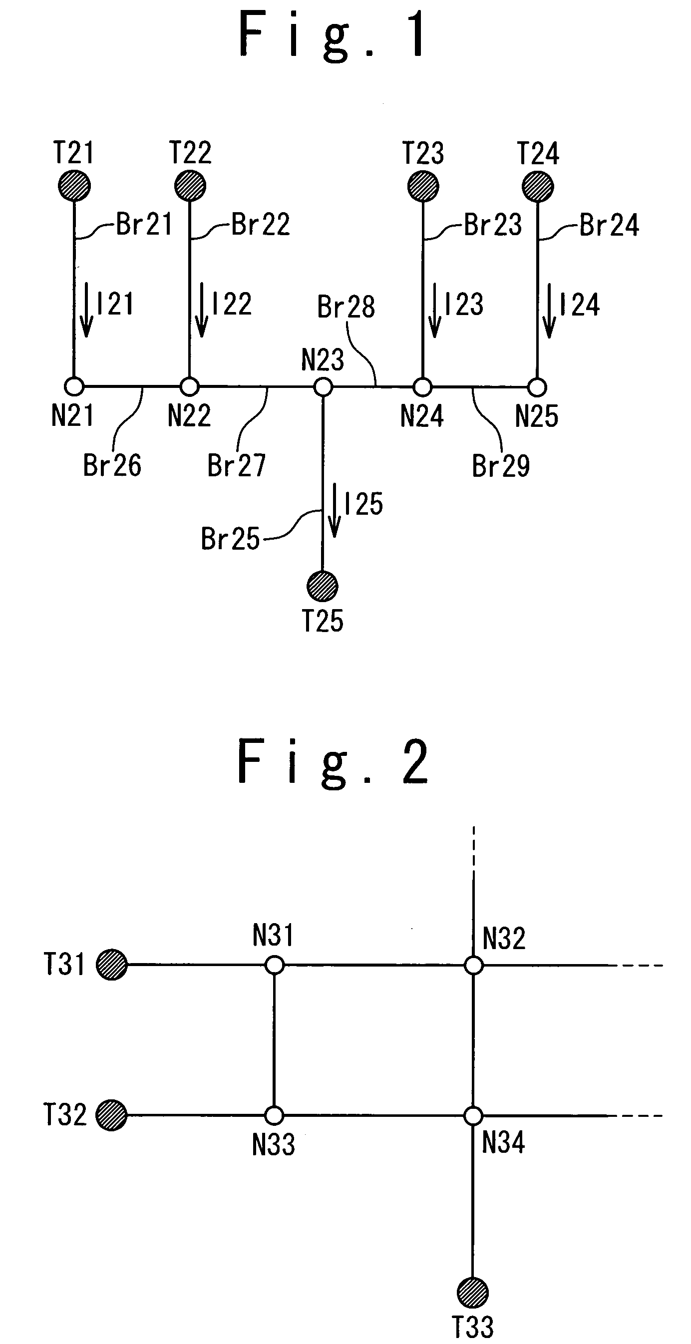
[0009] Therefore, an object of the present invention to provide a layout interconnections verifying apparatus and a method for verifying layout interconnections, which can obtain a current value of each branch interconnections in a short time, even if a loop portion is included in the interconnections.
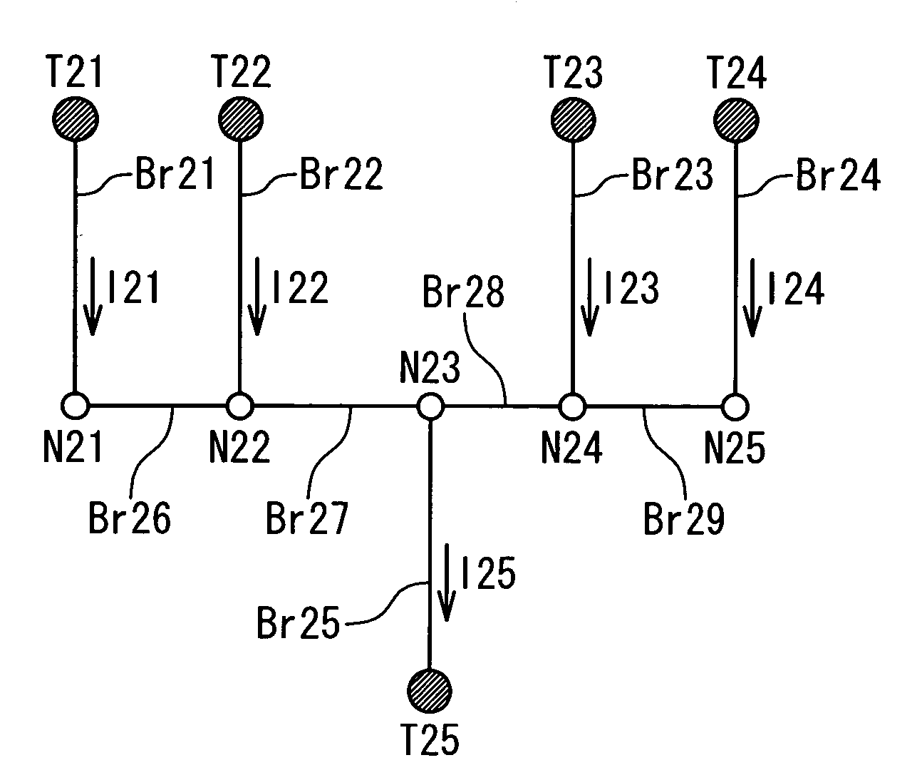
[0011] The layout interconnections verifying apparatus and the method for verifying layout interconnections of the present invention, when the loop is generated in the layout interconnections targeted for a verification, divides the whole into a portion that does not includes the loop and a portion that includes the loop, and calculates the current values. Thus, the current value of each branch interconnection can be easily obtained, thereby reducing the time necessary for the entire verification of the layout interconnections.

Problems solved by technology

However, this case has a problem that the calculation is complex which makes the time required to obtain the current value very long.

Method used


Image

  • Layout interconnections verifying apparatus and method for verifying layout interconnections
  • Layout interconnections verifying apparatus and method for verifying layout interconnections
  • Layout interconnections verifying apparatus and method for verifying layout interconnections

Examples


Embodiment Construction

[0024] Embodiments of a layout interconnections verifying apparatus and a method for verifying layout interconnections according to the present invention will be described below with reference to the attached drawings.

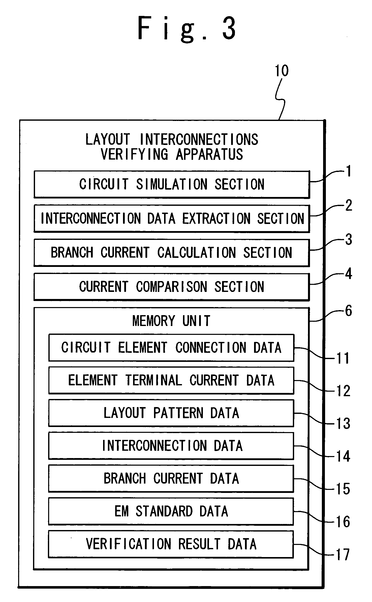
[0025]FIG. 3 is a view showing a configuration of the embodiment of a layout interconnections verifying apparatus according to the present invention. The layout interconnections verifying apparatus 10 is an information processing unit such as an workstation or an personal computer. The layout interconnections verifying apparatus 10 includes programs of a circuit simulation section 1, an interconnection data extraction section 2, a branch current calculation section 3 and a current comparison section 4, and stores data of circuit element (component) connection data 11, element terminal current data 12, layout pattern data 13, interconnection data 14, branch current data 15, EM standard data 16, and verification result data 17 in a memory unit 6.

[0026] The circuit simu...


PUM


Abstract

A method for verifying layout interconnections includes steps of (a) to (f). The step (a) extracts a loop circuit as a loop portion in a first circuit model. The first circuit model includes: branch interconnections which includes first branch interconnections included in the loop portion and other branch interconnections as second branch interconnections, first nodes, each of which is connected with an edge of corresponding one of the branch interconnections, and terminals of circuit elements, each of which is connected with an edge of corresponding one of the branch interconnections. The step (b) replacs the loop portion with a second node to generate a second circuit model which does not have a loop portion, based on the first circuit model. The step (c) calculats a second current value of each of the second branch interconnections, based on the second circuit model. The Sept (d) generates a third circuit model of the loop portion, based on the first interconnections. The step (e) calculates a first current value of each of the first branch interconnections, based on the third circuit model. The step (f) compares the first and second current value with a predetermined current value to carry out verification.

Description

BACKGROUND OF THE INVENTION [0001] 1. Field of the Invention [0002] The present invention relates to a layout interconnections verifying apparatus and a method for verifying layout interconnections. More particularly, the present invention relates to a layout interconnections verifying apparatus that can be used to judge whether or not layout interconnections satisfy a requirement with respect to a current based on whether or not a current flowing through each branch interconnection of the layout interconnections on a semiconductor device exceeds a predetermined current value, and a method for verifying layout interconnections that can do the same. [0003] 2. Description of the Related Art [0004] In a semiconductor device design, a layout of interconnections is designed after circuit elements such as transistors and the like are placed. After the layout of the interconnections, if the current flowing through the interconnection is locally concentrated and exceeds the predetermined cu...

Claims


Application Information

Patent Timeline
IPC IPC(8): G06F9/45G06F17/50H01L21/82
CPCG06F17/5022G06F30/33
Inventor TAKABE, TAKASHI
Owner RENESAS ELECTRONICS CORP
Learn More