
Nitride semiconductor light-emitting device and method for producing the same

a light-emitting device and semiconductor technology, applied in semiconductor/solid-state device manufacturing, semiconductor devices, electrical equipment, etc., can solve the problems of increasing power consumption, affecting the light-emitting efficiency per unit power, so as to reduce the injected carrier density, increase the light-emitting area, and increase the chip size

Active Publication Date: 2015-09-10
SHARP FUKUYAMA LASER CO LTD
View PDF7 Cites 6 Cited by
  • Summary
  • Abstract
  • Description
  • Claims
  • Application Information

AI Technical Summary

Benefits of technology

The present invention aims to produce a nitride semiconductor light-emitting device that prevents an increase in operation voltage and deterioration in light emission efficiency even at a large current, resulting in excellent power efficiency. The invention achieves this by decreasing the injected carrier density in the active layer, which reduces the likelihood of Auger recombination, carrier overflow, and deformation of the crystal structure. Additionally, the invention prevents an increase in the operation voltage and ensures stable operation at high current levels.

Problems solved by technology

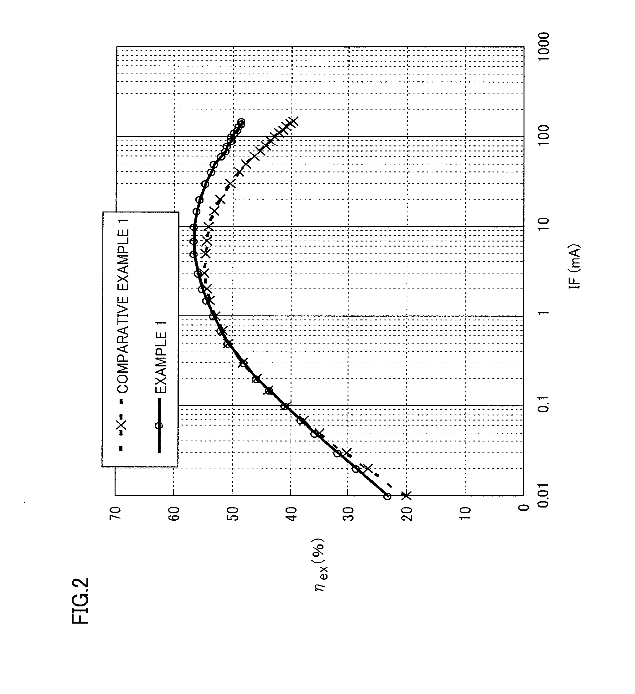
When a nitride semiconductor light-emitting device is produced according to the techniques as described in Japanese Patent Laying-Open No. 2005-109425 or Japanese Patent Laying-Open No. 2000-349337, and the produced nitride semiconductor light-emitting device is driven at a large current, the operation voltage can rise to lead increase in power consumption, and deterioration in light emission efficiency can be incurred.
From this, deterioration in light emission efficiency per unit power (power efficiency) can also be incurred.
It is generally believed that deterioration in light emission efficiency when the current density applied to a nitride semiconductor light-emitting device is relatively low is caused by a number of levels existing in the nitride semiconductor layer that induce non-light-emitting recombination (crystal defect and so on).
However, as the density of the current applied to the nitride semiconductor light-emitting device increases, it becomes difficult to improve the light emission efficiency only by decreasing crystal defects in the nitride semiconductor layer, and as the current density increases, a problem of decrease in light emission efficiency of the nitride semiconductor light-emitting device is incurred.
As a cause of such a problem, occurrence of non-light-emitting recombination in a layer other than the active layer is expected.
Therefore, it is difficult to prevent occurrence of non-light-emitting recombination.

Method used


Image

  • Nitride semiconductor light-emitting device and method for producing the same
  • Nitride semiconductor light-emitting device and method for producing the same
  • Nitride semiconductor light-emitting device and method for producing the same

Examples


first embodiment

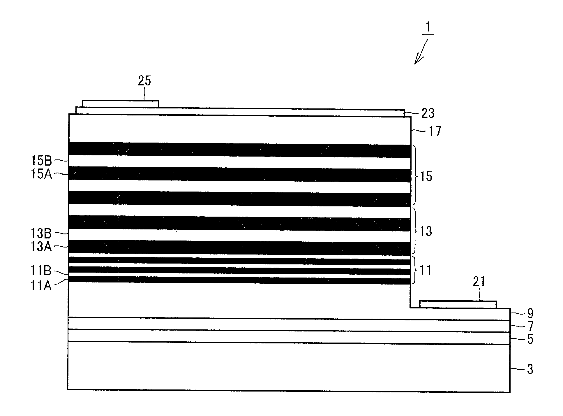
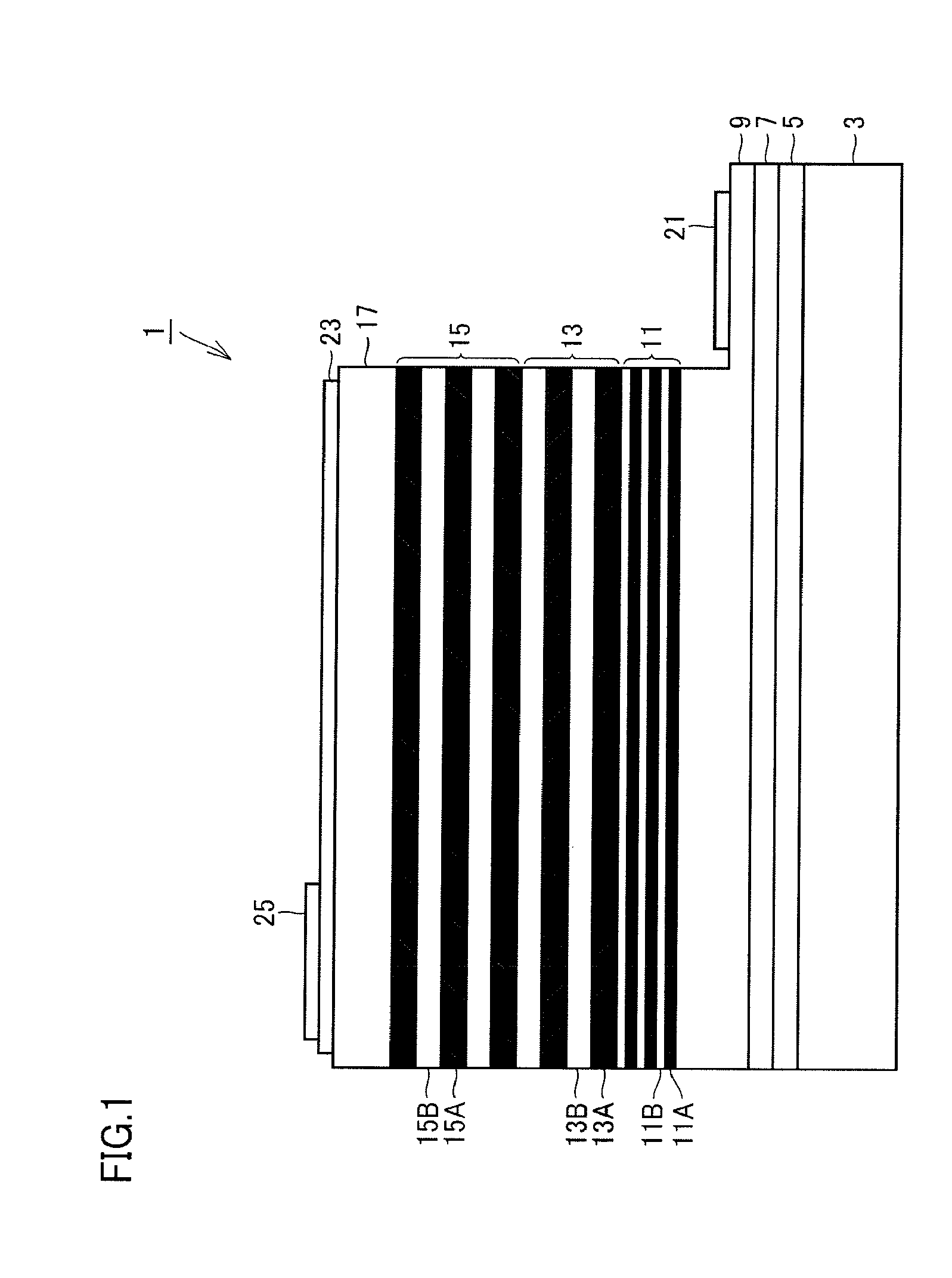
[0054]In a nitride semiconductor light-emitting device 1 according to the first embodiment of the present invention, an average carrier concentration of a long-period superlattice layer 13 is higher than an average carrier concentration of an active layer 15.

[0055]

[0056]Nitride semiconductor light-emitting device 1 according to the present embodiment is made up of a buffer layer 5, a base layer 7, an n-type nitride semiconductor layer 9, a short-period superlattice layer 11, long-period superlattice layer 13, active layer 15, and a p-type nitride semiconductor layer 17 stacked in this order on an upper face of a substrate 3. A part of an upper face of n-type nitride semiconductor layer 9 is exposed from short-period superlattice layer 11 and the like, and on the exposed part, an n-side electrode 21 is provided. On p-type nitride semiconductor layer 17, a p-side electrode 25 is provided with a transparent electrode 23 interposed therebetween.

[0057]

[0058]Substrate 3 may be, for exampl...

first modified example

[0129]In the first modified example, when both undoped layer 13B and well layer 15B do not contain an n-type impurity, the proportion of thickness per one layer of undoped layer 13B to thickness per one period of long-period superlattice layer 13 is made lower than the proportion of thickness per one layer of well layer 15B to thickness per one period of active layer 15. As a result, the proportion of a total volume of undoped layer 13B to a total volume of long-period superlattice layer 13 is lower than the proportion of a total volume of well layer 15B to a total volume of active layer 15. That is, the proportion of a total volume of layers not containing an n-type impurity to a total volume of long-period superlattice layer 13 is lower than the proportion of a total volume of layers not containing an n-type impurity to a total volume of active layer 15. As a result, the proportion of a total volume of layers containing an n-type impurity to a total volume of long-period superlatt...

second modified example

[0131]In the second modified example, concentration of the n-type impurity in doped layer 13A is higher than concentration of the n-type impurity in barrier layer 15A. As a result, the proportion of the ionized impurity is higher in doped layer 13A than in barrier layer 15A. Therefore, the average carrier concentration of long-period superlattice layer 13 is higher than the average carrier concentration of active layer 15.

[0132]Concentration of the n-type impurity in doped layer 13A is preferably more than once concentration of the n-type impurity in barrier layer 15A. Preferably, concentration of the n-type impurity in doped layer 13A is greater than or equal to 1.2 times and less than or equal to 1000 times concentration of the n-type impurity in barrier layer 15A, or less than or equal to 2×1019 cm−3. When concentration of the n-type impurity in doped layer 13A is less than once concentration of the n-type impurity in barrier layer 15A, it can be difficult to make the average car...


PUM

PropertyMeasurementUnit
flatnessaaaaaaaaaa
Lengthaaaaaaaaaa
flatnessaaaaaaaaaa

Abstract

A nitride semiconductor light-emitting device has a first conductive-type nitride semiconductor layer, a superlattice layer provided on the first conductive-type nitride semiconductor layer, an active layer provided on the superlattice layer, and a second conductive-type nitride semiconductor layer provided on the active layer. An average carrier concentration of the superlattice layer is higher than an average carrier concentration of the active layer.

Description

[0001]This is a continuation application of U.S. application Ser. No. 13 / 533,649, filed Jun. 26, 2012, which is a nonprovisional application based on Japanese Patent Application No. 2011-145900, filed Jun. 30, 2011, the entire contents of which are hereby incorporated by reference.BACKGROUND OF THE INVENTION[0002]1. Field of the Invention[0003]The present invention relates to a nitride semiconductor light-emitting device and a method for producing the same.[0004]2. Description of the Background Art[0005]Conventionally, a nitride semiconductor light-emitting device usable for a light-emitting diode or the like is known. In such a nitride semiconductor light-emitting device, when a voltage is applied, an electron and a hole are recombined in an active layer, and as a result, light is generated. The active layer may have a single quantum well structure, or may have a multiple quantum well structure as described in Japanese Patent Laying-Open No. 2005-109425 and Japanese Patent Laying-O...

Claims


Application Information

Patent Timeline
Patent Type & Authority Applications(United States)
IPC IPC(8): H01L33/06H01L33/32H01L33/22
CPCH01L33/06H01L2933/0033H01L33/32H01L33/22H01L33/04
Inventor FUDETA, MAYUKOKOMADA, SATOSHIKAIHARA, RYU
Owner SHARP FUKUYAMA LASER CO LTD
Learn More