Vertical type bipolar transistor manufacture method and vertical type bipolar transistor

A technology of bipolar transistors and manufacturing processes, applied in semiconductor/solid-state device manufacturing, semiconductor devices, electrical components, etc., can solve the problems of high manufacturing cost, complicated process, and complicated manufacturing technology, and achieve lower precision requirements, lower costs, The effect of process simplification

Inactive Publication Date: 2008-06-04
SHANGHAI HUA HONG NEC ELECTRONICS
View PDF0 Cites 10 Cited by
  • Summary
  • Abstract
  • Description
  • Claims
  • Application Information

AI Technical Summary

Problems solved by technology

In practical applications, vertical bipolar transistors are generally used more, but their manufacturing technology is also more complicated than that of horizontal bipolar transistors.
The current advanced vertical bipolar transistor manufacturing process technology mainly uses two polysilicon electrodes (double-poly) and self-alignment process, but when using the above process meth

Method used


Image

  • Vertical type bipolar transistor manufacture method and vertical type bipolar transistor
  • Vertical type bipolar transistor manufacture method and vertical type bipolar transistor
  • Vertical type bipolar transistor manufacture method and vertical type bipolar transistor

Examples


Example Embodiment

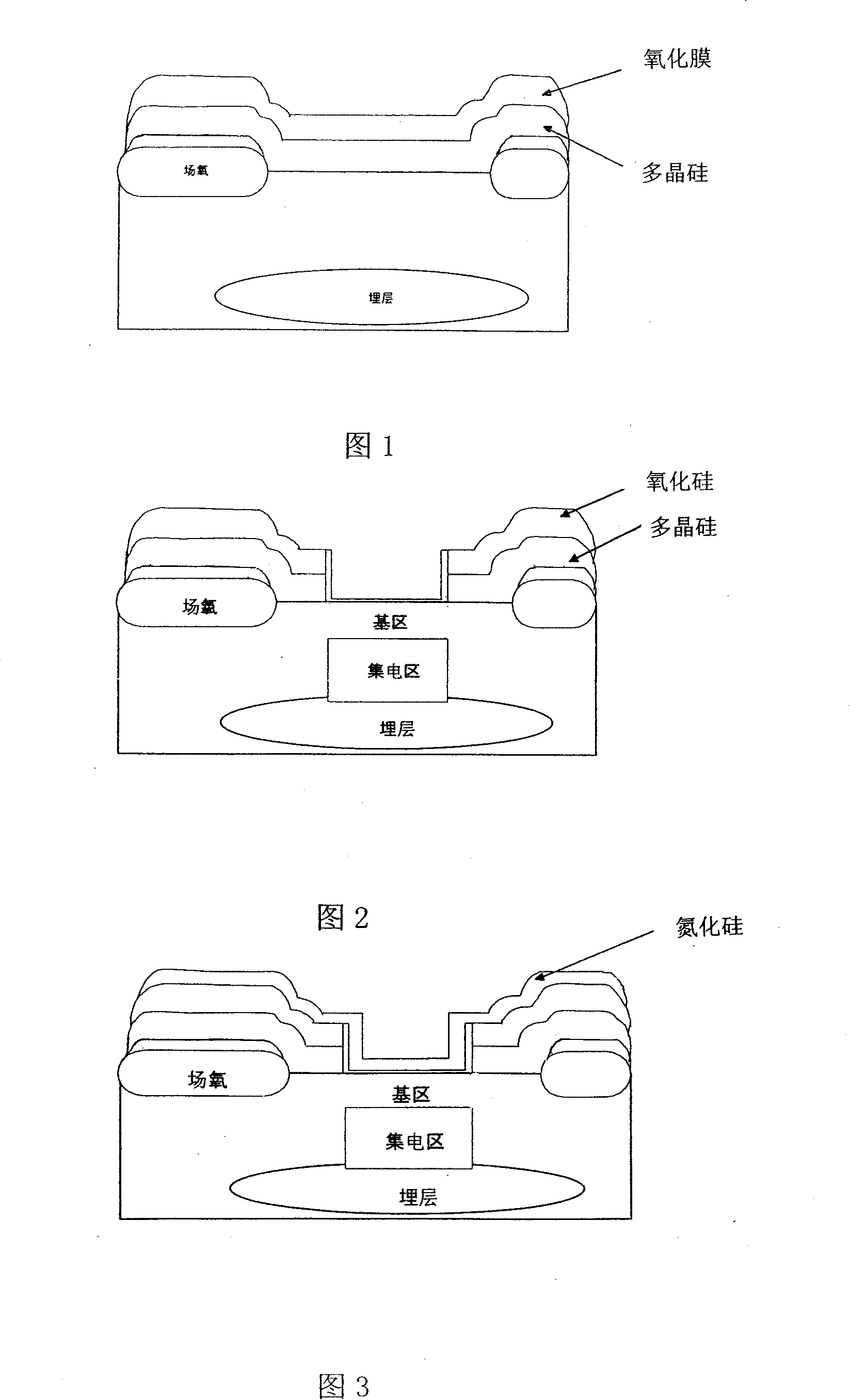
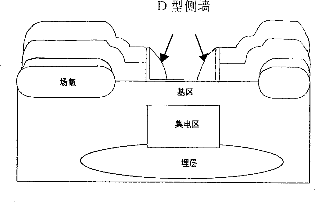
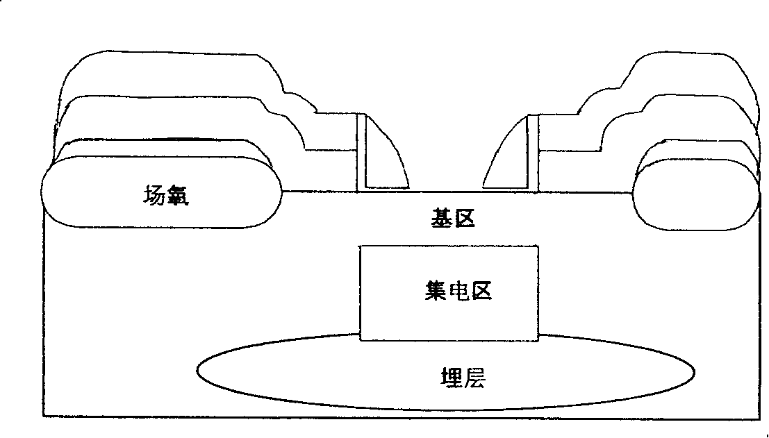
[0012] The preparation method of the vertical bipolar transistor of the present invention adopts a D-shaped sidewall structure and a self-aligning process to form the emitter of a small-size vertical bipolar transistor. The D-shaped sidewall is also used to isolate the external Base and emitter. The specific process flow is as follows:

[0013] First, a layer of polysilicon is deposited on the P-type silicon substrate, and a thicker (about 2000 angstroms) oxide film is deposited on the polysilicon layer (see FIG. 1). The deposition method can adopt common chemical vapor deposition or other methods to form the polysilicon layer. The specific methods for forming the polysilicon layer, the nitride film layer, etc., described in the following steps of the present invention can be achieved by various methods known in the prior art.

[0014] The ion implantation area is formed by photolithography and etching, and the ion implantation area is used as the emission area of ​​the preset ver...


PUM


Abstract

The invention discloses a method for manufacturing technics of a bipolar transistor with vertical type and a bipolar transistor with vertical type. The method comprises the following steps: after ion implantation is carried out to obtain an intrinsic base region and a collector region which is under the intrinsic base region, a buffer layer is further deposited; the buffer layer is etched by a single-step dry method to form a side wall; a wet method is adopted to etch and wipe off the film to expose the intrinsic base region; emitter heteromorphic silicon is deposited; an emitter is obtained by chemical wet etching; then an external base is formed by using chemical wet etching again. The invention guarantees the dimensional precision of the emitter, and at the same time has a low requirement for the precision of an etching plate. The invention is simple in technics and cost-efficient.

Description

technical field [0001] The invention relates to a manufacturing process method of a semiconductor transistor device, in particular to a manufacturing process method of a vertical bipolar transistor. The invention also relates to a vertical bipolar transistor made by the method. Background technique [0002] Bipolar transistors are one of the device structures that make up modern large-scale integrated circuits. The advantages of bipolar transistors are fast operation speed, large output current per unit chip area, and small change in on-state voltage, which is suitable for making analog circuits; the disadvantages are small input resistance, large power consumption, and complicated process. [0003] There are various types of structures of bipolar transistors, for example, lateral bipolar transistors, vertical bipolar transistors (such as vertical bipolar transistors), and so on. In practical applications, more vertical bipolar transistors are generally used, but their man...

Claims


Application Information

Patent Timeline
IPC IPC(8): H01L21/331H01L29/732
Inventor 李永海
Owner SHANGHAI HUA HONG NEC ELECTRONICS
Why Eureka
Try Eureka