Laser processing apparatus, laser processing method, manufacturing method of wiring substrate, manufacturing method of display apparatus and wiring substrate

一种激光加工方法、激光加工的技术,应用在激光焊接设备、金属加工设备、制造工具等方向,能够解决长生产周期、工艺复杂等问题,达到提高制造产量、改善特性、简单和可靠激光加工的效果

Inactive Publication Date: 2008-06-11
SONY CORP
View PDF3 Cites 3 Cited by
  • Summary
  • Abstract
  • Description
  • Claims
  • Application Information

AI Technical Summary

Problems solved by technology

As a result, it is necessary to cut other regions by laser to eliminate the influence of the interlayer short section and the process is complicated
[0012] As mentioned above, the correction methods according to the prior art are technically complex and have other disadvantages such as long production cycles

Method used


Image

  • Laser processing apparatus, laser processing method, manufacturing method of wiring substrate, manufacturing method of display apparatus and wiring substrate
  • Laser processing apparatus, laser processing method, manufacturing method of wiring substrate, manufacturing method of display apparatus and wiring substrate
  • Laser processing apparatus, laser processing method, manufacturing method of wiring substrate, manufacturing method of display apparatus and wiring substrate

Examples


example

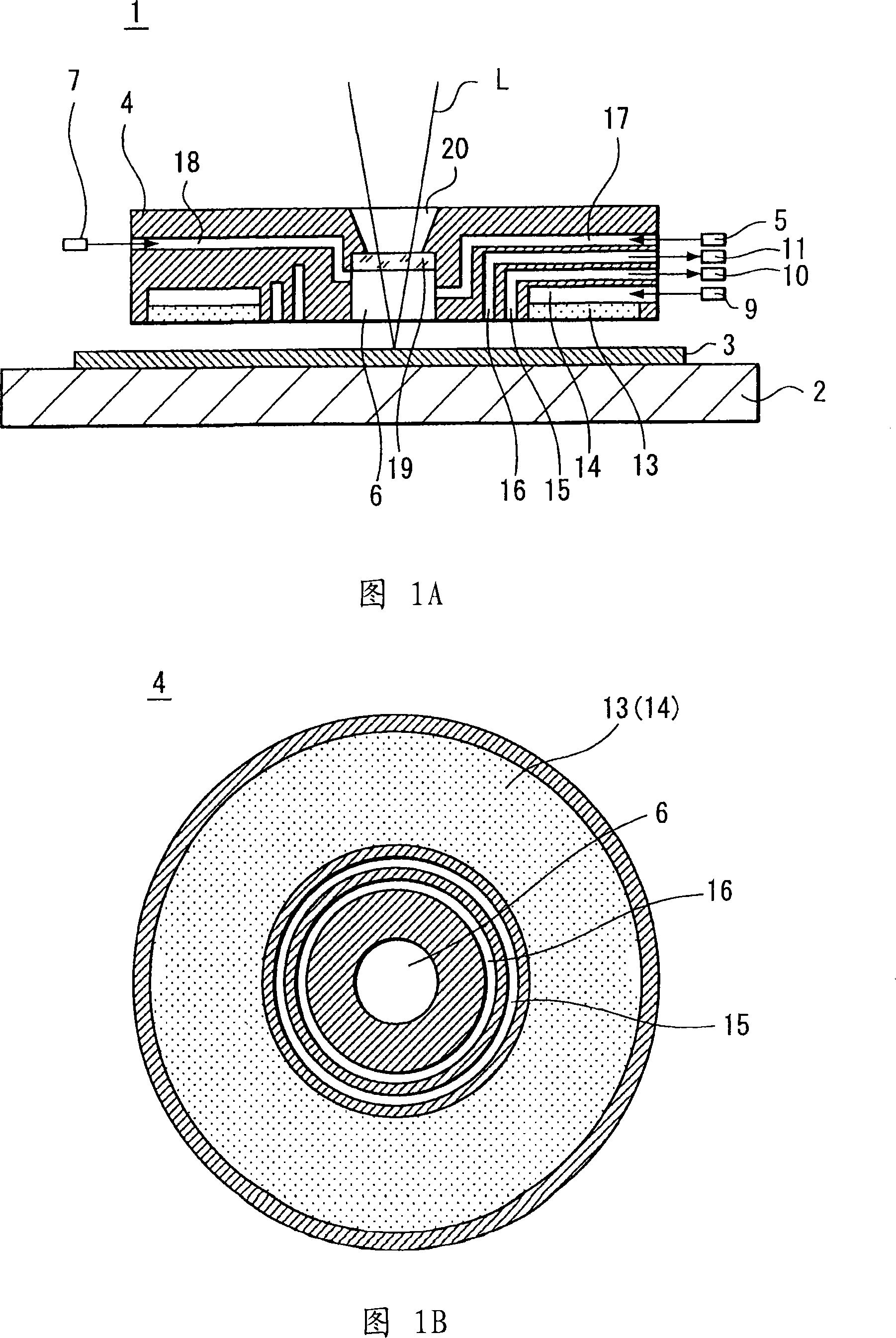
[0097] An example (detection result) of a wiring substrate (array substrate) manufacturing method is described below as a specific example of a laser processing method according to an embodiment of the present invention.

[0098] With the apparatus shown in FIGS. 1A and 1B , a thin film transistor (TFT) substrate was used as a processing object and laser processing was performed.

[0099] First, the inert gas argon (Ar) or nitrogen (N 2 ) is injected into the support table 2 through the porous gas permeable membrane 13 inside the local exhaust 4. The local exhaust device 4 is raised above the thickness of the processed object 3 , for example, 100 μm away from the support table 2 . Therefore, even when the processing object 3 is slightly bent or shaken, the local exhaust device 4 and the processing object 3 can avoid contacting each other in the next process.

[0100] Next, the support table 2 is moved in the horizontal direction and the processing object 3 is inserted into t...


PUM


Abstract

The invention discloses a laser processing apparatus, laser processing method, manufacturing method of wiring substrate, manufacturing method of display apparatus. A laser processing apparatus includes a support table, a local exhaust device, and a laser light source unit. The support table supports a processing object. The local exhaust device directs laser light into a local exhaust unit in which pressure is locally adjusted over the support table. The laser light source unit outputs the laser light. The local exhaust device is capable of relatively being lifted from the support table by injecting a lift gas to the support table. The processing object includes a multilayer film formed of two or more layers with different materials. An input unit into which reflectance of the processing object is inputted is connected to the laser light source unit.

Description

technical field [0001] The present invention relates to a laser processing device, a laser processing method executable using the laser processing device, a method of manufacturing a wiring substrate using the laser processing method, a method of manufacturing a display device including the wiring substrate, and A wiring board obtained by this laser processing method. Background technique [0002] A structure produced on the assumption of mass production has a predetermined structural pattern determined for the purpose. This structure may be a wiring substrate or a photomask including components (wires, etc.) and devices (capacitors, etc.). Also, a structure including a wiring substrate and using a photomask in a manufacturing process may be a display device such as a flat panel display (FPD). [0003] However, predetermined patterns may be incompletely formed on these structures during fabrication and features and devices are often observed to be overformed (e.g., extendi...

Claims


Application Information

Patent Timeline
Patent Type & Authority Applications(China)
IPC IPC(8): B23K26/40C23C16/00H01L21/768
CPCC23C16/45517C23C16/45519C23C16/483Y10T428/31
Inventor 下田和人舆石亮冨冈聪川部英雄
Owner SONY CORP
Why Eureka
Try Eureka