Method for eliminating leftover after chemical mechanical grinding

A chemical mechanical and residue technology, which is applied in the fields of polishing compositions containing abrasives, electrical components, semiconductor/solid-state devices, etc., can solve the problems of pollutant residue, achieve high grinding rate, improve reliability and stability , cheap effect

Inactive Publication Date: 2008-06-11
SEMICON MFG INT (SHANGHAI) CORP +1
View PDF1 Cites 22 Cited by
  • Summary
  • Abstract
  • Description
  • Claims
  • Application Information

AI Technical Summary

Problems solved by technology

[0005] Therefore, the object of the present invention is to provide a method for removing residues after chemical mechanical grinding, to solve the existing problem of residual pollutants after grinding the wafer surface containing tungsten

Method used


Image

  • Method for eliminating leftover after chemical mechanical grinding
  • Method for eliminating leftover after chemical mechanical grinding
  • Method for eliminating leftover after chemical mechanical grinding

Examples


Embodiment Construction

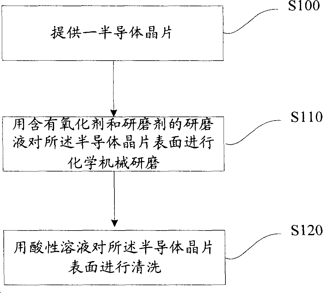
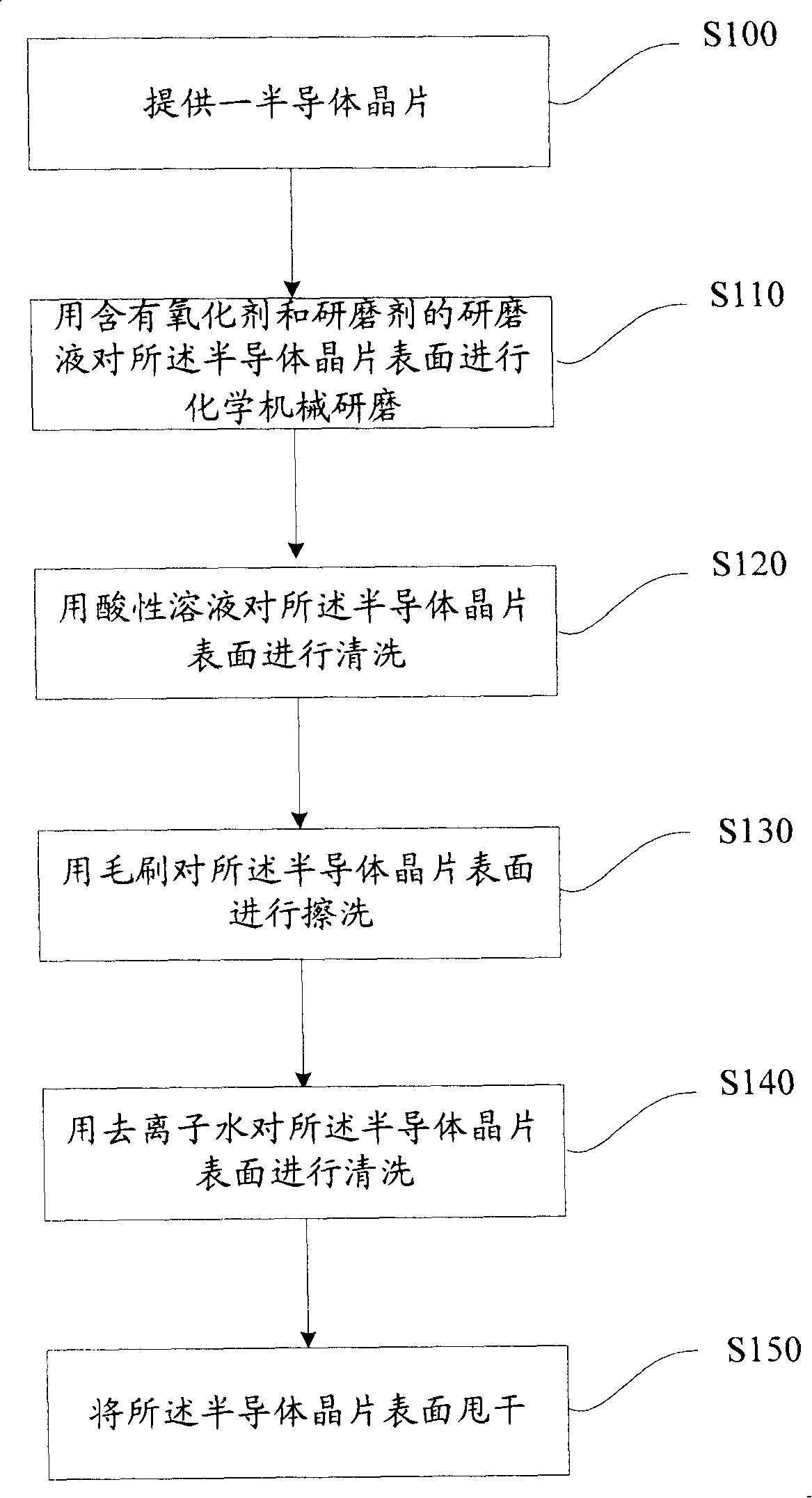
[0029] In order to make the above objects, features and advantages of the present invention more comprehensible, specific implementations of the present invention will be described in detail below in conjunction with the accompanying drawings.

[0030] In the semiconductor manufacturing process, tungsten is often used as a connection plug to connect the semiconductor transistor device and the metal interconnection line at the back end. The process of forming the connection plug is generally a damascene process, that is, firstly, a contact hole (contact) is formed in the insulating dielectric layer through a photolithography and etching process, and then metal tungsten is deposited in the contact hole, and is planarized by chemical mechanical polishing. liquefied, followed by post-grind cleaning to remove slurry and particle contamination. The invention provides a method for removing residues after chemical mechanical grinding of tungsten, which can effectively remove residues ...


PUM


Abstract

The invention relates to a removing method for residue after chemical and mechanical grinding, which comprises the following steps of: providing a semi-conductor wafer; performing chemical and mechanical grinding for the surface of the semi-conductor wafer by using a grinding solution containing oxidizer and grinding agent; and cleaning the surface of the semi-conductor by acidity solution. The method can remove the grinded pollutant residue.

Description

technical field [0001] The invention relates to the technical field of semiconductor manufacturing, in particular to a method for removing residues after chemical mechanical polishing of tungsten. Background technique [0002] With the increasing reduction of semiconductor devices, the excessive fluctuation of the wafer surface due to the deposition process of multi-layer interconnection or filling aspect ratio causes the difficulty of focusing in the lithography process, which weakens the ability to control the line width and reduces the overall To ensure the uniformity of the line width on the wafer, the industry introduces chemical mechanical planarization (CMP) to planarize the wafer surface. The steps are as follows: place the silicon wafer on a grinding head, and make the surface of the silicon wafer downwardly contact with a polishing pad, and then planarize the surface of the silicon wafer by the relative movement between the surface of the silicon wafer and the poli...

Claims


Application Information

Patent Timeline
Patent Type & Authority Applications(China)
IPC IPC(8): H01L21/302H01L21/306H01L21/321H01L21/3213C09G1/02
Inventor 张斐尧李福洪杜应提薛景星
Owner SEMICON MFG INT (SHANGHAI) CORP
Why Eureka
Try Eureka