Pholithography and wafer forming by the same

A chip and photoresist technology, applied in the field of photolithography process, can solve the problems of tin ball pollution sealing ring, electroplating sealing ring is not tightly sealed, etc., to achieve the effect of improving production efficiency, ensuring sealing, reducing cleaning frequency and time

Inactive Publication Date: 2008-06-18
SEMICON MFG INT (SHANGHAI) CORP
View PDF0 Cites 11 Cited by
  • Summary
  • Abstract
  • Description
  • Claims
  • Application Information

AI Technical Summary

Problems solved by technology

[0005] The object of the present invention is to provide a new photolithography process and the wafer formed by the photolithography process, which can effectively

Method used


Image

  • Pholithography and wafer forming by the same
  • Pholithography and wafer forming by the same

Examples


Embodiment Construction

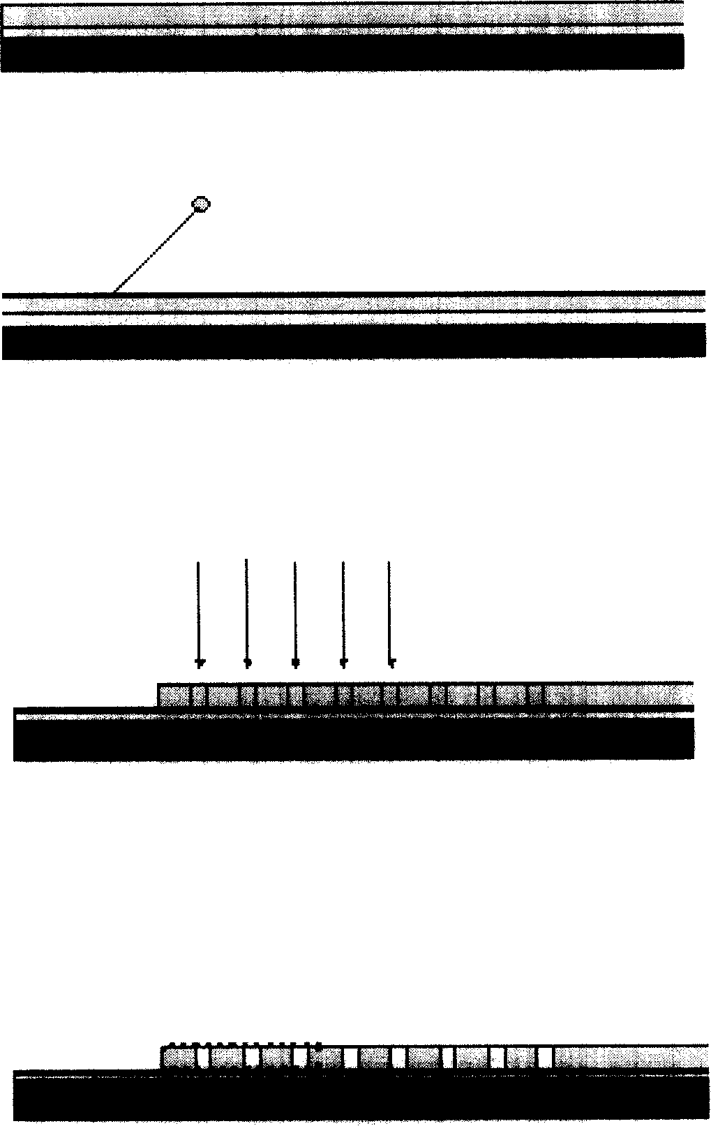
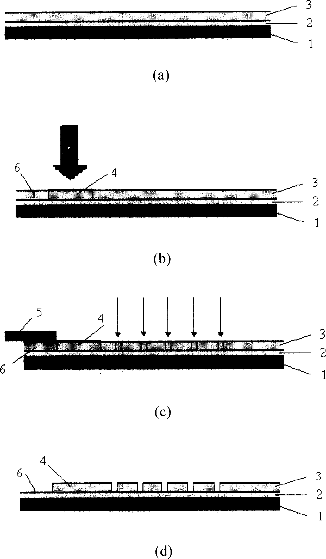
[0012] see figure 2 , The photolithography process of the present invention includes four steps of gluing, wafer edge exposure, exposure and development.

[0013] see figure 2 (a) is a schematic diagram of applying glue to the wafer 1 . Before entering the photolithography process, the surface of the wafer 1 has been covered with a layer of metal dielectric layer 2 , and the wafer 1 is coated with glue, that is, a layer of photoresist 3 is covered on the metal dielectric layer 2 of the wafer 1 .

[0014] see figure 2 (b), is a schematic diagram of wafer 1 edge exposure. The area 4 of the wafer 1 that may contact the sealing ring (not shown) is exposed. In the embodiment of the present invention, the width of the edge of the wafer 1 is about 1.3 mm. The width of the edge protection area 6 of the wafer 1 is approximately 1.2 mm, so the contact area 4 between the sealing ring and the wafer 1 is approximately 1.2 mm to 2.5 mm away from the edge of the wafer 1 .

[0015] se...


PUM


Abstract

The invention provides a photoetching manufacture procedure. Firstly, the metal medium layer on the surface of the chip is coated with photoresist and the chip is arranged in a plating cavity for plating after finished the photoetching manufacture procedure; the plating cavity is provided with a sealing ring and an electrode inside, wherein, the manufacture procedure also comprises the following steps: a. the selected area of the edge of the chip is exposed; b. the protective area of the edge of the chip is kept off with a baffle object and then cannot be affected by exposure; c. a special picture is adopted to expose the chip and the special picture is provided with a hole with internal so that the photo resistance on the surface of the chip can be exposed with interval; d. the chip conducts development and the unexposed photo resistance is melted. The photoetching manufacture procedure of the invention firstly exposes the selected area of the edge of the chip contacted with the sealing ring after gelatinizing and the selected area of the edge directly contacted with the sealing ring has no photoetching image, therefore, airtight of the sealing ring is ensured; in addition, pollutant cannot be generated in the process of plating to pollute the sealing ring and production efficiency is effectively improved.

Description

technical field [0001] The invention relates to a semiconductor manufacturing process, in particular to a photolithographic manufacturing process. Background technique [0002] In the semiconductor manufacturing process, the photolithography process is first performed to form a photolithography pattern on the surface of the wafer, and then enters the electroplating process to grow solder balls on the wafer. In the electroplating process, the entire wafer is placed in an electroplating chamber and then placed in an electroplating solution for electroplating. An electrode and a sealing ring are arranged in the electroplating chamber. When the wafer is placed in the electroplating chamber, the electrodes are in contact with the metal medium layer on the edge of the wafer for conduction; the sealing ring is used to prevent the electroplating solution from penetrating into the metal medium layer on the edge of the wafer. [0003] When the wafer enters the photolithography proces...

Claims


Application Information

Patent Timeline
IPC IPC(8): G03F7/20H01L21/027C25D5/02C25D7/12
Inventor 李德君
Owner SEMICON MFG INT (SHANGHAI) CORP
Why Eureka
Try Eureka