Manufacturing process for cleaning Flash chip
A chip and cleaning solution technology, applied in the field of Flash chip manufacturing process, can solve problems such as affecting the data retention capability of storage devices, and achieve the effect of preventing cross-contamination
- Summary
- Abstract
- Description
- Claims
- Application Information
AI Technical Summary
Problems solved by technology
Method used
Image

Examples
Embodiment Construction
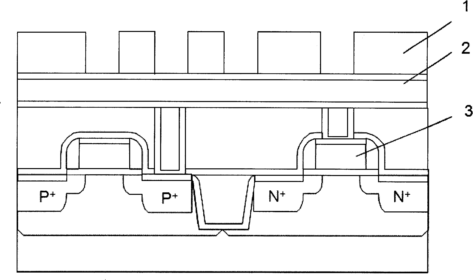
[0010] see figure 1 The Flash chip of the present invention includes a metal layer 1 , a dielectric layer 2 and a storage device 3 . The dielectric layer 2 is used to isolate the metal layer 1 and the storage device 3 .
[0011] In the flash chip cleaning process of the present invention, the chip is cleaned with a single-chip cleaning machine, and the cleaning liquid is drained after cleaning a chip and will not be reused.
[0012] The cleaning solution in the process of the present invention is a water-based cleaning solution. The cleaning solution used in the preferred embodiment of the present invention is weak alkaline cleaning solution ST250.
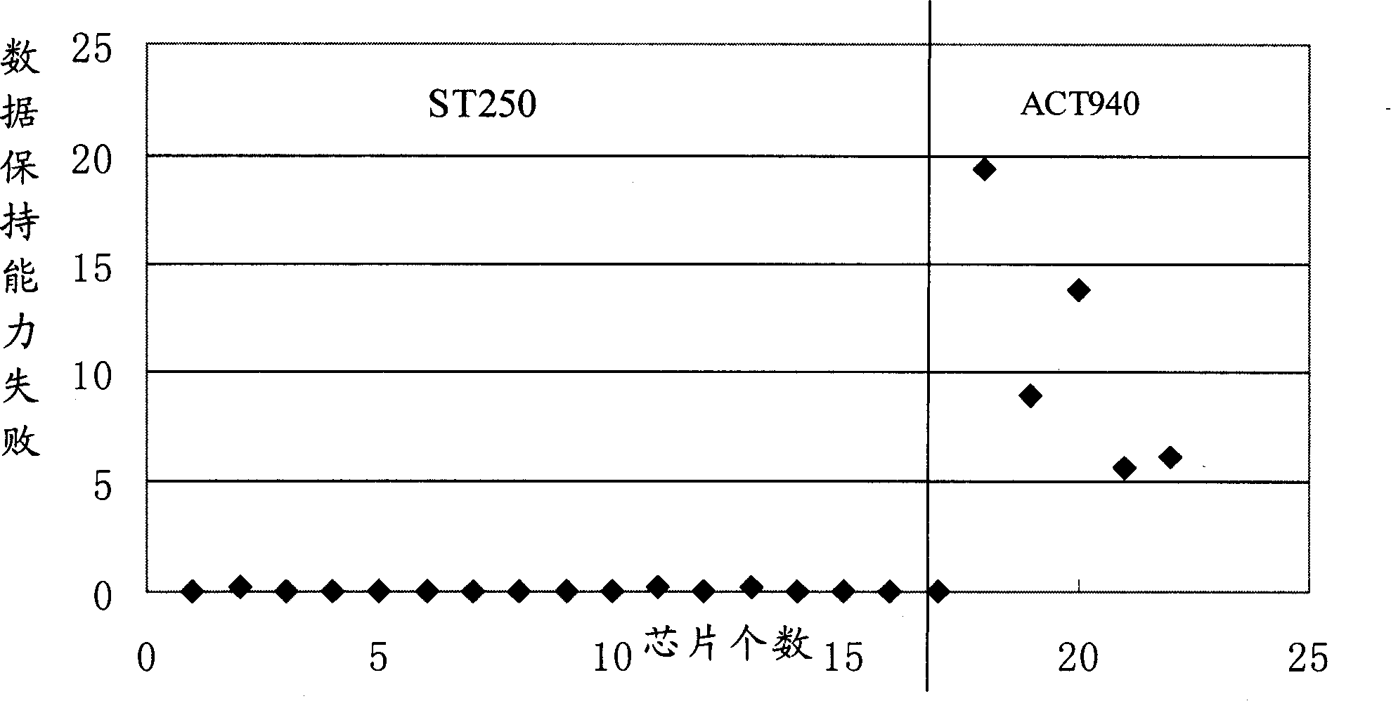
[0013] see figure 2 , the left side of the chart is the test result of cleaning with a single-chip cleaning machine with a weak alkaline cleaning solution ST250, and the right side is the test result of using a multi-chip cleaning machine with an alkaline cleaning solution ACT940 in the prior art . The abscissa is the number...
PUM
 Abstract
Description
Claims
Application Information
 - R&D
- Intellectual Property
- Life Sciences
- Materials
- Tech Scout
- Unparalleled Data Quality
- Higher Quality Content
- 60% Fewer Hallucinations
Browse by: Latest US Patents, China's latest patents, Technical Efficacy Thesaurus, Application Domain, Technology Topic, Popular Technical Reports.
© 2025 PatSnap. All rights reserved.Legal|Privacy policy|Modern Slavery Act Transparency Statement|Sitemap|About US| Contact US: help@patsnap.com