Method for forming shallow trench isolation

A technology of shallow grooves and grooves, which is applied in the direction of electrical components, semiconductor/solid-state device manufacturing, circuits, etc., can solve the problems of easy contamination of semiconductor substrates, and achieve the effects of saving consumption, improving stability, and reducing costs

Inactive Publication Date: 2008-06-25
SEMICON MFG INT (SHANGHAI) CORP
View PDF1 Cites 24 Cited by
  • Summary
  • Abstract
  • Description
  • Claims
  • Application Information

AI Technical Summary

Problems solved by technology

[0011] Therefore, the object of the present invention is to provide a method for forming shallow trench isolation, to solve the problem that the semiconductor substrate is exposed to the external environment for many times and is easily polluted in the existing manufacturing method of shallow trench isolation.

Method used


Image

  • Method for forming shallow trench isolation
  • Method for forming shallow trench isolation
  • Method for forming shallow trench isolation

Examples


Embodiment Construction

[0035] In order to make the above objects, features and advantages of the present invention more comprehensible, specific implementations of the present invention will be described in detail below in conjunction with the accompanying drawings.

[0036] Figure 6 It is a flow chart of the first embodiment of the manufacturing method of the shallow trench isolation of the present invention.

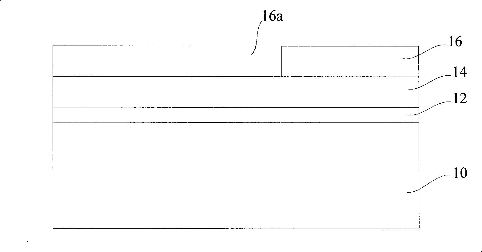
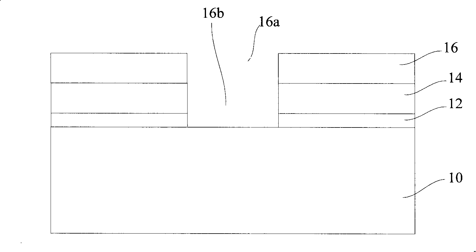
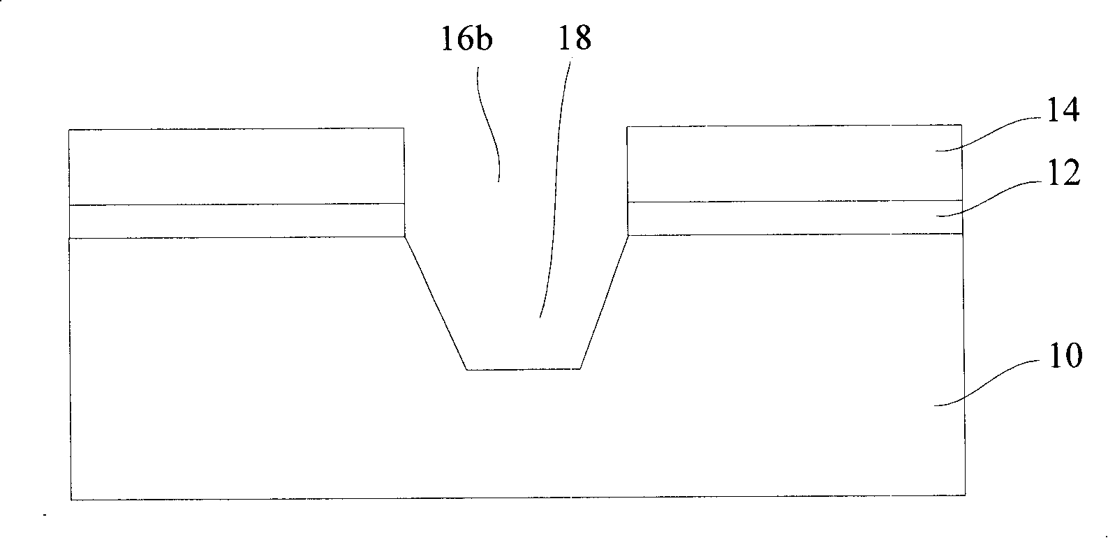
[0037] Such as Figure 6 As shown, a semiconductor substrate having a trench is provided (S100). The material of the semiconductor substrate may be single crystal silicon or polycrystalline silicon, and the semiconductor substrate may also include a silicon-on-insulator structure, a silicon germanium compound, a silicon gallium compound, and the like.

[0038] The trench in the semiconductor substrate can be formed by the following steps:

[0039] First, an oxide layer is grown on the semiconductor substrate through a thermal oxidation process as a pad oxide layer (PadOxide), and the thi...


PUM


Abstract

The invention relates to a shallow groove isolation formation method. The method comprises the following steps: a semiconductor substrate with a groove is provided; pad oxide layers are formed on the bottom part and the side wall of the groove, and in situ annealing is performed; insulation substance is filled into the groove. The shallow groove isolation formation method of the invention can reduce the transmission frequency of the substrate, reduce the pollution, ensures the process to be simplified, and reduces the cost.

Description

technical field [0001] The invention relates to the technical field of semiconductor manufacturing, in particular to a method for forming shallow trench isolation in a semiconductor manufacturing process. Background technique [0002] As the semiconductor manufacturing process develops to a process node with a small line width, the isolation process between semiconductor devices has also been developed from an early local oxidation process (LOCOS) to a shallow trench isolation (Shallow Trench Isolation, STI) process. The main steps of the shallow trench isolation process are: trench etching, insulator filling, grinding and planarization. Since the shallow trench isolation process directly affects the leakage current and other electrical properties between semiconductor devices on the semiconductor substrate, the industry always uses various methods to improve the performance of the shallow trench isolation. Chinese patent application No. 200410101523.1 discloses a method fo...

Claims


Application Information

Patent Timeline
Patent Type & Authority Applications(China)
IPC IPC(8): H01L21/762
Inventor 何有丰白杰朴松源
Owner SEMICON MFG INT (SHANGHAI) CORP
Why Eureka
Try Eureka