Method for forming device isolation region

A technology of device isolation and wet etching, applied in semiconductor/solid-state device manufacturing, electrical components, circuits, etc., can solve the problems of polysilicon layer residue, word line short circuit, etc., to maintain height and reduce static leakage current.

Inactive Publication Date: 2008-06-25
SEMICON MFG INT (SHANGHAI) CORP +1
View PDF1 Cites 14 Cited by
  • Summary
  • Abstract
  • Description
  • Claims
  • Application Information

AI Technical Summary

Problems solved by technology

Since the memory cell area is a device-dense area, the shallow trench width used for active device isolation is generally 0.10um to 0.20um, so the depth of the depression is very small, almost zero; but the peripheral circuit area is a non-dense area of ​​active devices , some shallow trenches have a width of 0.3um to 20um, and after polishing the insulating oxide layer in shallow trenches of this width, the depth of the depression is 0.03um to 0.04um; when the

Method used


Image

  • Method for forming device isolation region
  • Method for forming device isolation region
  • Method for forming device isolation region

Examples


Embodiment Construction

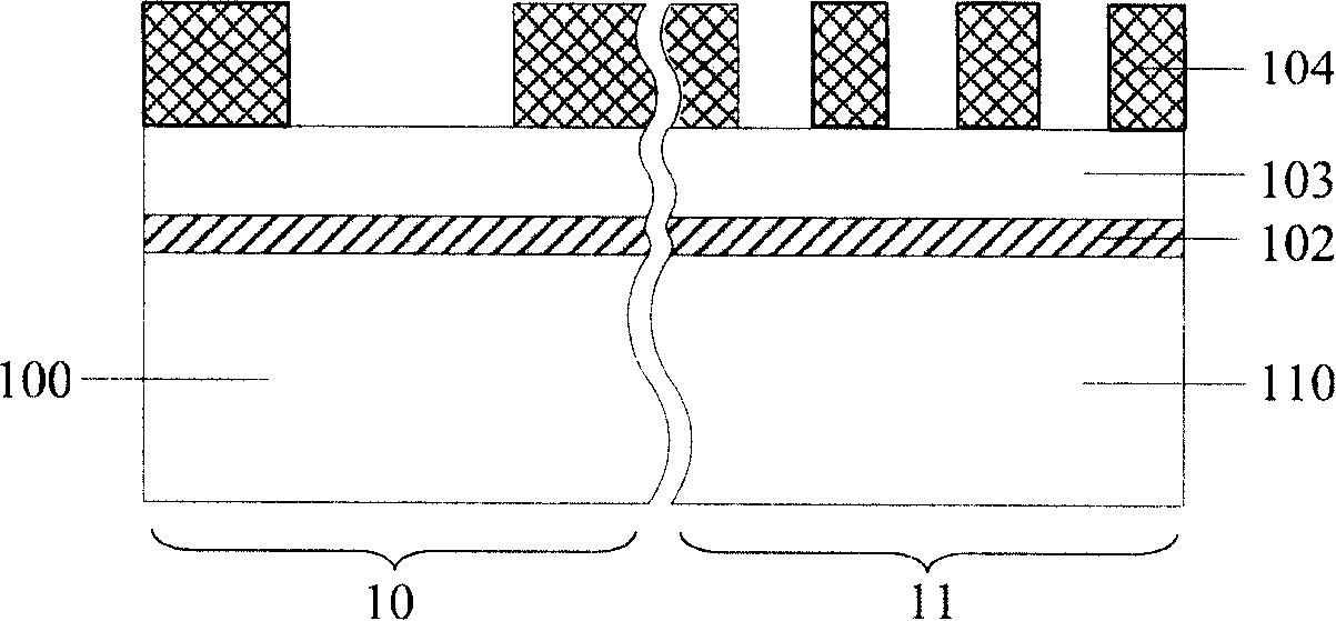
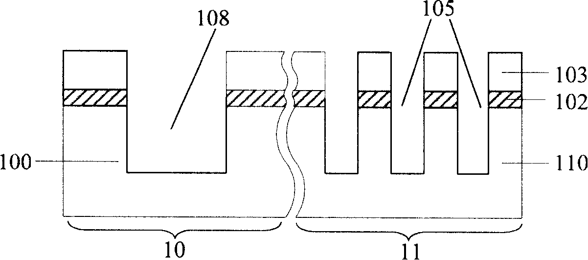
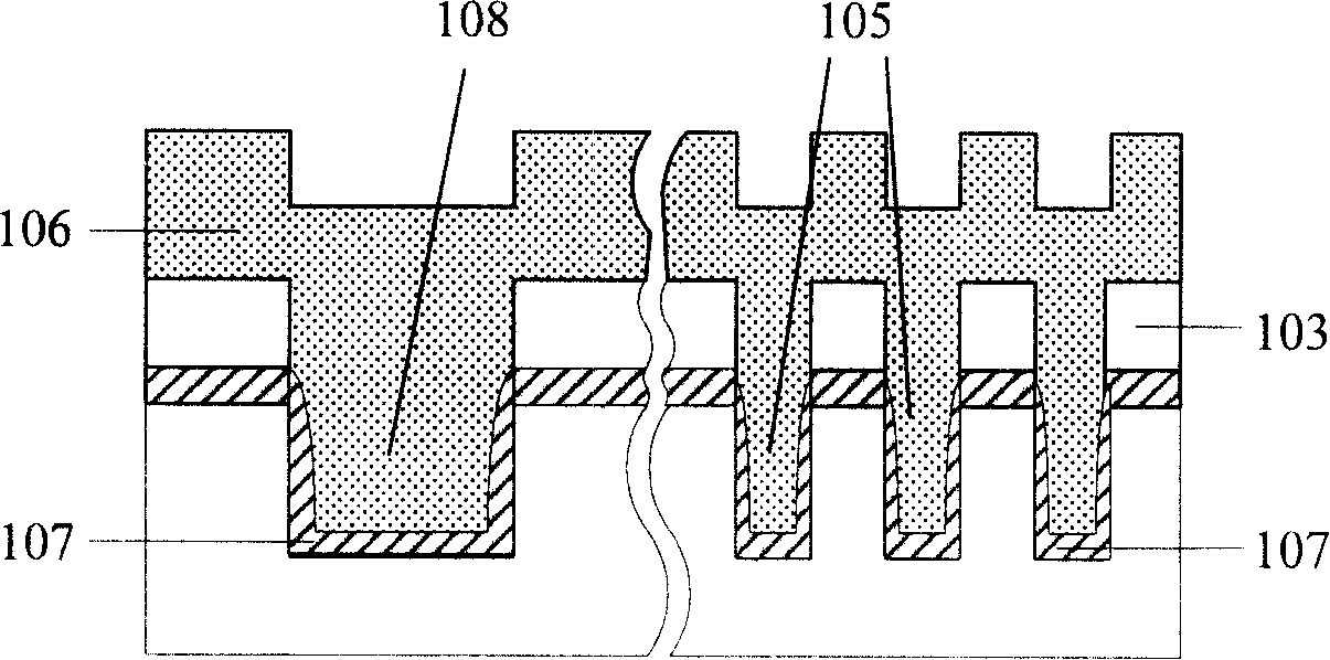
[0019] As the semiconductor technology enters the deep submicron era, the active area isolation of devices below 0.18 μm has mostly been produced by shallow trench isolation technology. Shallow trench isolation technology is an effective method to solve the "bird's beak" problem caused by local oxidation isolation in MOS circuits. In the existing process of manufacturing the shallow trench isolation structure, since the insulating oxide layer in the shallow trench is lower than the insulating oxide layer on the silicon nitride layer after the deposition of the insulating oxide layer, the insulating oxide layer is polished to the silicon nitride layer. When the silicon nitride layer is over-polished to ensure that the insulating oxide layer on the silicon nitride layer is completely removed, when the silicon nitride layer is over-polished, the insulating oxide layer in the shallow trench will also be removed. During grinding, since the rate of grinding the silicon nitride layer...


PUM

PropertyMeasurementUnit
Thicknessaaaaaaaaaa

Abstract

The invention relates to a formation method of a device isolation area. The method comprises the following steps: a silicon substrate comprising a peripheral circuit area and a storage unit area is provided; a pad oxide layer and a silicon nitride layer are formed on the silicon substrate in sequence; the pad oxide layer, the silicon nitride layer and the silicon substrate are etched to form a groove; an insulating oxide layer is formed on the silicon nitride layer, and the insulating oxide layer is filled into the groove; the insulating oxide layer is grounded until the silicon nitride layer is exposed; photoresist is formed on the peripheral circuit area; the photoresist is taken as a mask, the insulating oxide layer in the storage unit area is etched until the height is coincident with the height of the insulating oxide layer in the peripheral circuit area; the photoresist, the silicon nitride layer and the pad silicon oxide layer are removed, so as to form a shallow groove isolation structure. The height of shallow groove isolation structure of the storage unit is reduced through the said steps, the phenomenon that the shallow groove isolation structure of the storage unit area generates excessive grinding is avoided during the subsequent planarization process of the polysilicon layer, and the phenomenon that the residues of the polysilicon layer is generated during the etching process of the subsequent word line of the storage unit to result in the word line short circuit is also avoided.

Description

technical field [0001] The invention relates to a method for forming a device isolation region, in particular to a method for manufacturing a shallow trench isolation semiconductor device. Background technique [0002] As the size of integrated circuits decreases, the devices that make up the circuits must be placed more densely to fit the limited space available on the chip. Since current research is devoted to increasing the density of active devices per unit area of ​​a semiconductor substrate, effective insulating isolation between circuits becomes more important. The methods for forming isolation regions in the prior art mainly include local oxidation isolation (LOCOS) process or shallow trench isolation (STI) process. The LOCOS process is to deposit a layer of silicon nitride on the surface of the silicon substrate, and then perform etching to oxidize and grow silicon oxide in part of the recessed area, and the active device is generated in the area determined by the ...

Claims


Application Information

Patent Timeline
IPC IPC(8): H01L21/762H01L21/822
Inventor 蔡信裕刘经国陈荣堂孙智江
Owner SEMICON MFG INT (SHANGHAI) CORP
Why Eureka
Try Eureka