Method for forming of via hole

A technology of pore size and hole opening, applied in the field of through-hole formation, can solve the problems of limited adjustment range, limited pore size, poor controllability, etc., and achieve the effect of simple and convenient size, large pore size range, and strong controllability

Active Publication Date: 2008-06-25
SEMICON MFG INT (SHANGHAI) CORP +1
View PDF1 Cites 10 Cited by
  • Summary
  • Abstract
  • Description
  • Claims
  • Application Information

AI Technical Summary

Problems solved by technology

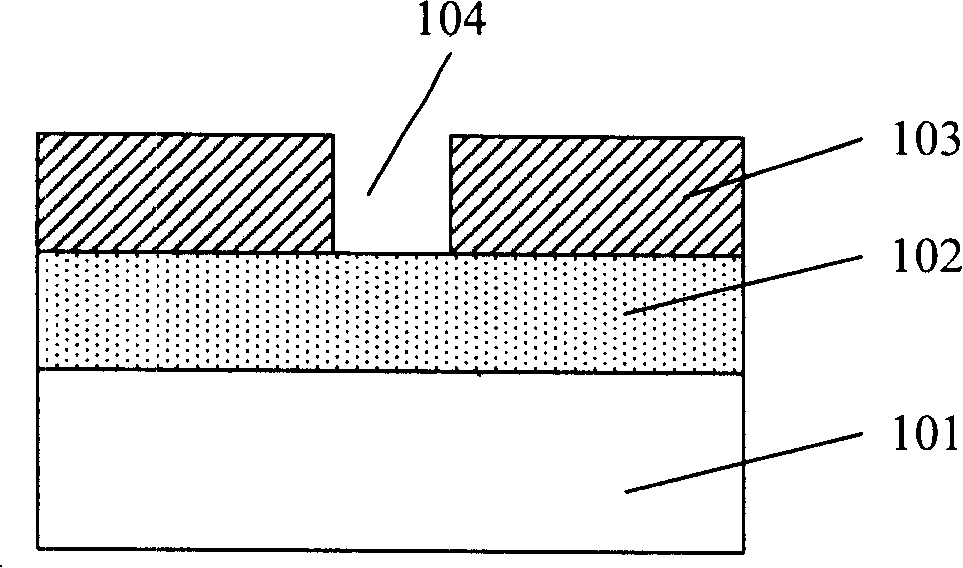
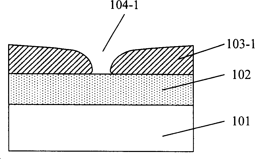
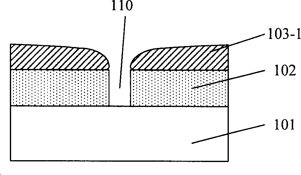
[0007] 1. The shape of the photoresist after thermal reflow depends on the size of its pattern. The inconsistency of the pattern size in the chip will lead to different degrees of photoresist reflow. As a result, the aperture of each hole formed by etching under its protection will not be the same uniform;
[0008] 2. The expansion of the photoresist after thermal reflow is limited in the horizontal dimension. Therefore, the aperture of the through hole that can be formed by it is also limited compared with the exposure size during photolithography, and the adjustable aperture size is limited;
[0009] 3. The shape of the photoresist after thermal reflow will be irregular, resulting in poor edge shape and sidewall shape of the formed small-aperture through hole (not shown in the figure)
[0010] 4. The thermal reflow of photoresist is not easy to control accurately, and the controllability of aperture adjustment is poor
Due to the uncertainty of thermal reflow of photoresist, the through holes formed by this method also have problems such as uneven size, limited adjustment range, poor shape, poor controllability, etc., and the quality of the formed holes is poor

Method used


Image

  • Method for forming of via hole
  • Method for forming of via hole
  • Method for forming of via hole

Examples


Embodiment Construction

[0048] In order to make the above objects, features and advantages of the present invention more comprehensible, specific implementations of the present invention will be described in detail below in conjunction with the accompanying drawings.

[0049] The processing method of the present invention can be widely applied in many applications, and can utilize many suitable materials to make, and below is to illustrate by preferred embodiment, certainly the present invention is not limited to this specific embodiment, this field Common replacements known to those skilled in the art undoubtedly fall within the protection scope of the present invention.

[0050] Secondly, the present invention is described in detail using schematic diagrams. When describing the embodiments of the present invention in detail, for the convenience of explanation, the cross-sectional view showing the device structure will not be partially enlarged according to the general scale, which should not be used...


PUM


Abstract

The invention discloses a formation method ofa through hole. The method comprises the following steps: a substrate is provided; photoetching processing is performed to the substrate to form a hole pattern with a first aperture; an additional dielectric layer is deposited; the substrate is etched, and a through hole with a second aperture is formed on the substrate. Through adopting the formation method of the invention, the formed through hole has the advantages that the size is even, the shape is regular, the adjustable range of the aperture is larger than usual, the controllability is higher, and the formation quality is higher.

Description

technical field [0001] The invention relates to the technical field of semiconductor manufacturing, in particular to a method for forming a through hole. Background technique [0002] The process of manufacturing semiconductor integrated circuit chips uses batch processing technology to form a large number of various types of complex devices on the same silicon substrate and connect them to each other to have complete electronic functions. With the rapid development of ultra-large-scale integrated circuits, the integration of chips is getting higher and higher, and the size of components is getting smaller and smaller. The various effects caused by the high density and small size of devices have an increasing impact on the results of semiconductor process manufacturing. protrude. A typical example is the production of small-aperture through-holes: as the size of the device shrinks, the size of the various holes that need to be formed in chip manufacturing is further reduced...

Claims


Application Information

Patent Timeline
IPC IPC(8): H01L21/768H01L21/02H01L21/311
Inventor 杜珊珊韩秋华张世谋
Owner SEMICON MFG INT (SHANGHAI) CORP
Why Eureka
Try Eureka