Pattern shielding structure for dry etching and method thereof

A technology of electronic packaging and electronic components, applied in the direction of electrical components, electrical solid devices, circuits, etc., can solve the problems of increased chances of telecommunication interference, increased distribution density of integrated circuit chips, and affecting the signal stability of electronic products, etc.

Active Publication Date: 2008-06-25
群成能源股份有限公司
View PDF2 Cites 13 Cited by
  • Summary
  • Abstract
  • Description
  • Claims
  • Application Information

AI Technical Summary

Problems solved by technology

This patent mainly uses a plurality of via holes 206 to be formed in the chip, and at the same time, a metallization line 204 is laid on the hole wall, and a fixed structure 205 with conductive properties is used, so it can effectively shorten the telecommunications transmission path between chips and reduce signal noise. Although the packaging structure can shorten the transmission path between chips, due to the increase in the distribution density of integrated circuit chips, the chances of telecommunication interference between different types of chips will increase, which will affect the stability of electronic product signals

Method used


Image

  • Pattern shielding structure for dry etching and method thereof
  • Pattern shielding structure for dry etching and method thereof
  • Pattern shielding structure for dry etching and method thereof

Examples


Embodiment Construction

[0069] The foregoing and other objects, features, and advantages of the present invention will be more clearly understood through the following detailed description with reference to the illustrated preferred embodiments.

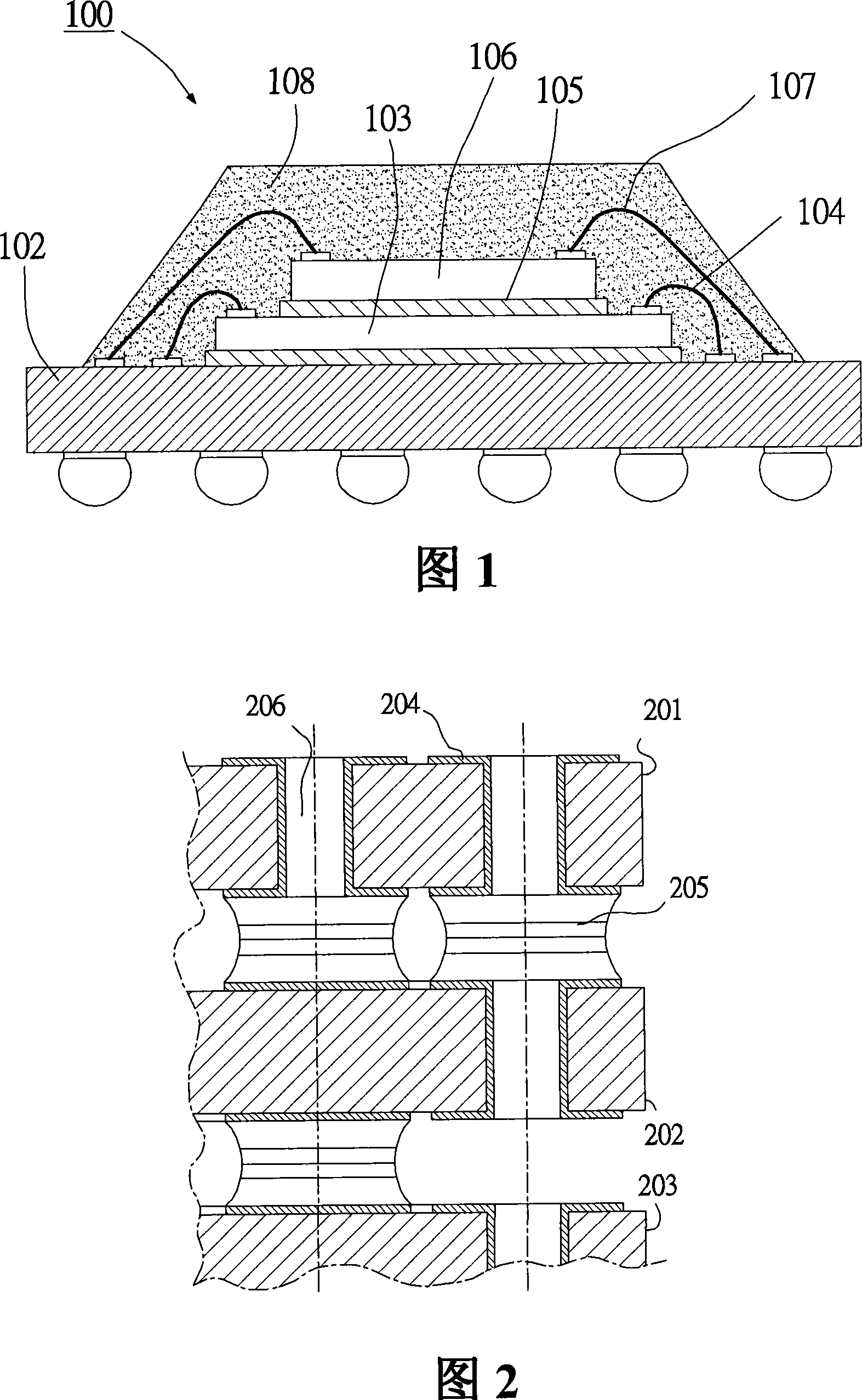
[0070] The invention discloses an electronic packaging structure. Specifically, the present invention proposes a three-dimensional stacked packaging unit with enhanced grounding characteristics. The packaging unit can achieve the purpose of multi-chip stacking through the telecommunication contacts on both sides. The detailed description of the embodiment of the invention is as follows, but the preferred embodiment described is only for illustration and is not intended to limit the present invention.

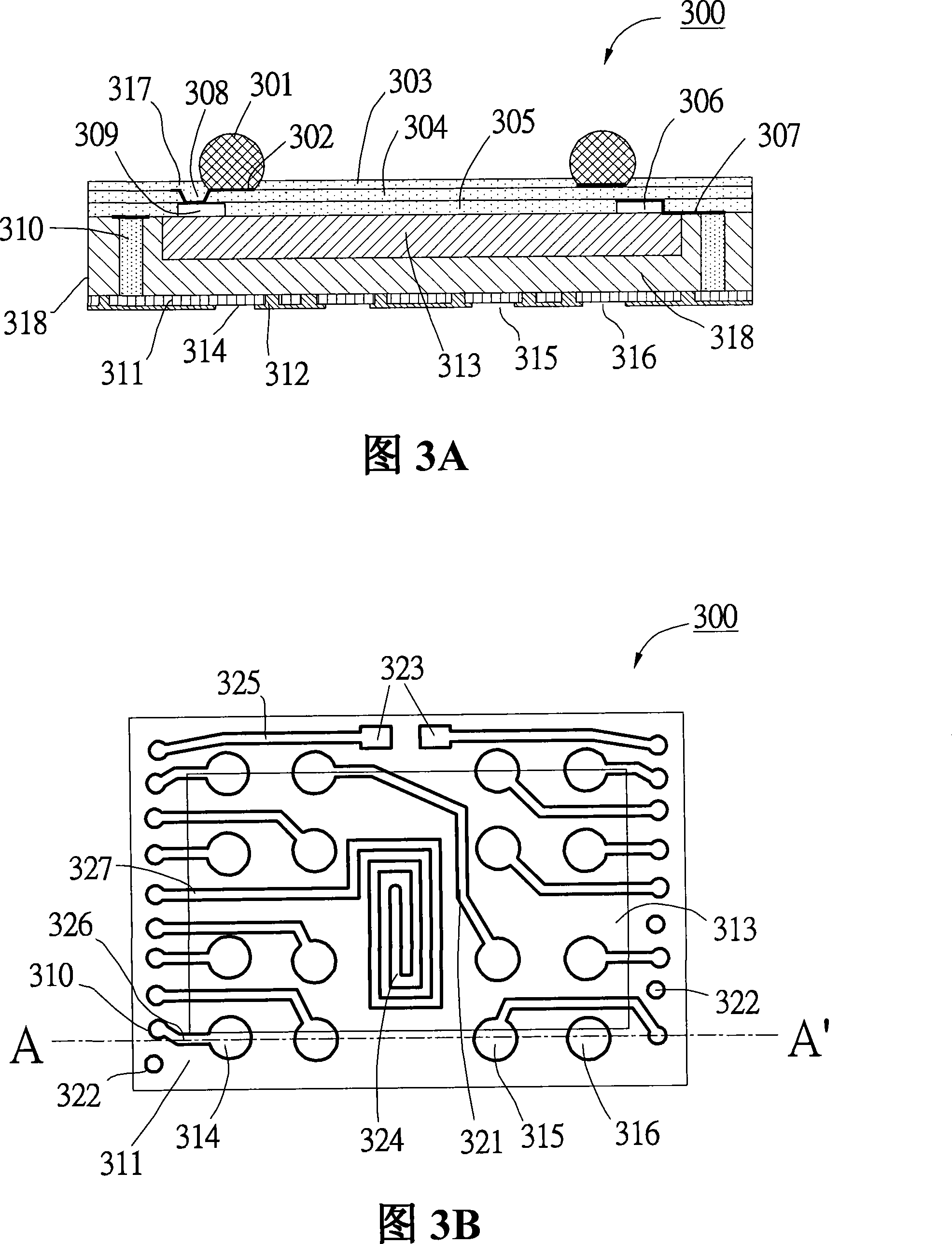
[0071] Fig. 3A is a sectional view of the first packaging unit 300 of the present invention, which is also the A-A' section in Fig. 3B. In the figure, the electronic component substrate 318 can be composed of silicon, germanium, tin, carbon, or a combination...


PUM


Abstract

The present invention proposes a 3D electronic packaging structure with enhanced grounding performance and embedded antenna, and the packaging unit can achieve multi-chip stacking through the signal contacts on the top and bottom surfaces of the unit. A single or multiple grounding layers are on the back of the substrate in the packaging unit to facilitate the grounding for the semiconductor element; further, the packaging unit is applicable to a wafer level packaging process, so the manufacturing cost of each individual packaging unit is reduced. The above grounding layers are also the signal transmission paths of the electronic elements in the packaging structure of the invention, and a single or multiple via holes around the electronic element layers allow electrical signal connection between the top and bottom surfaces of the packaging structure, and thus enable more functionality in the packaging unit. Moreover, the grounding layers may have circular signal channels to construct a 3D stacked packaging structure with embedded antenna.

Description

technical field [0001] The present invention relates to an electronic packaging structure, especially a three-dimensional stacked packaging unit with enhanced grounding characteristics and embedded antennas. The telecommunication contacts on both sides of the packaging unit achieve the purpose of multi-chip stacking. Background technique [0002] Today's electronic products are mostly aimed at miniaturization, high performance, high precision, high reliability, and high responsiveness, etc., so that the distribution density of circuit components is too high, and the volume of the circuit is greatly reduced. However, the circuits of electronic products are more delicate. There will be more and more components formed in a small space, so the chance of mutual telecommunication interference will increase, affecting the stability of electronic product signals; among them, electromagnetic interference (Electromagnetic Interference, EMI) and noise are the most common problems. The...

Claims


Application Information

Patent Timeline
Patent Type & Authority Applications(China)
IPC IPC(8): H01L23/488H01L23/538
CPCH01L2924/01032H01L2225/1058H01L2224/18H01L23/3128H01L2924/01004H01L2924/01045H01L2224/32245H01L2924/01002H01L2225/1005H01L2924/15311H01L2924/01029H01L2924/01027H01L23/552H01L25/16H01L2224/48091H01L2924/19015H01L2924/01013H01L2224/32225H01L2924/15331H01L2924/01047H01L24/48H01L2225/1035H01L2924/01079H01L25/105H01L24/18H01L2224/48227H01L2924/14H01L2924/01005H01L2924/01033H01L2224/32145H01L2924/01006H01L2924/01074H01L2924/01078H01L2924/01075H01L2223/6677H01L2224/73265H01L2924/3025H01L2924/1461H01L2924/181H01L2924/00014H01L24/19H01L24/97H01L2224/04105H01L2224/12105H01L24/20H01L2924/00015H01L2924/00H01L2924/00012H01L2224/45099H01L2224/45015H01L2924/207H01L23/12
Inventor 游明志邱建嘉江国宁杨文焜
Owner 群成能源股份有限公司
Why Eureka
Try Eureka