High voltage MOS device

A MOS device, high-voltage technology, applied in the direction of semiconductor devices, electrical components, circuits, etc., can solve the problems of slow speed, increase breakdown voltage, and small safe working area, so that the speed of the device is not affected, the breakdown voltage is improved, The effect of a large safe working area

Inactive Publication Date: 2008-07-09
GRACE SEMICON MFG CORP
View PDF0 Cites 13 Cited by
  • Summary
  • Abstract
  • Description
  • Claims
  • Application Information

AI Technical Summary

Problems solved by technology

Among them, Figure 1(a) is an ordinary LDMOS, and Figure 1(b) is an LDMOS using gate polysilicon 13 as a field plate. This structure improves the breakdown voltage and reduces the on-resistance. The disadvantage is that the speed is not fast, and it works safely. small area
[0005] Figure 1(c) is a MOS device in which the field plate 17 and the source 11 are connected together. This structure also increases the breakdown voltage, and the speed is not affected. The disadvantage is that the on-resistance is increased

Method used


Image

  • High voltage MOS device
  • High voltage MOS device

Examples


Embodiment Construction

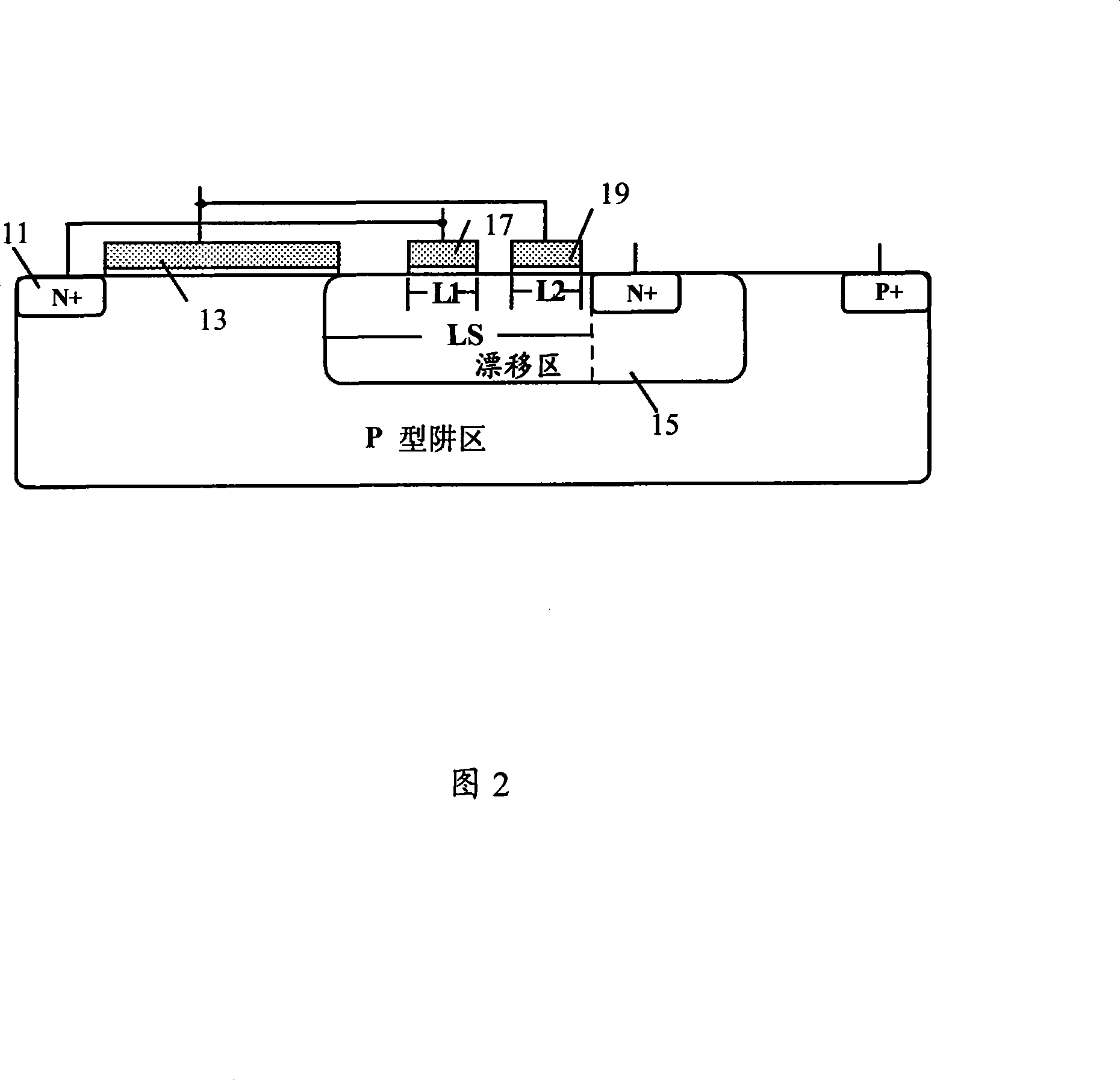
[0018] The present invention proposes a high-voltage MOS device, please refer to FIG. 2 , the device at least includes a source 11 , a gate 13 , a drift region 15 , a first field plate 17 and a second field plate 19 . Both the first field plate 17 and the second field plate 19 are made of a polysilicon layer with the same thickness as the polysilicon layer of the gate 13 , and are distributed on the upper surface of the drift region 15 at a distance from each other. Wherein, the first field plate 17 closest to the gate 13 is connected to the source 11 , and the second field plate 19 is connected to the gate 13 .

[0019] The lengths L1 and L2 of the two field plates 17 and 19 can be the same or different, and the lengths L1 and L2 range from the minimum value allowed by the process to about one-third of the length LS of the drift region 15, which can be determined according to different high-voltage MOS devices. Choose from different lengths ranging from 1 micron to 100 micron...


PUM


Abstract

The invention provides a high-voltage MOS device, which at least includes a grid, a source and a drift region, wherein, the device further includes at least two field plates which are mutually separated with certain distance and are distributed at the upper surface of the drift region, the field plate which is nearest to the grid is connected with the source, and the other field plate is connected with the grid. The two field plates are both composed of polysilicon layers, and the thickness is the same as the thickness of the polysilicon layers. The lengths of the two filed plates can be same or different. The length of the field plate is decided by the doping level of the drift area, the lower the doping level of the drift area is, the longer the filed plate is, and the length of the filed plate is not more than one third of the length of the drift region. The length of the field plate is more than one sixth and less than one fourth of the length of the drift region. Compared with the prior art, the device of the invention can improve breakdown voltage and reduce on-resistance, the speed of the device is not affected and safe working area is larger.

Description

technical field [0001] The invention relates to a high-voltage MOS device, in particular to a high-voltage MOS device. Background technique [0002] The application of high-voltage MOS devices is more and more extensive. Evaluating the performance of high-voltage devices generally includes three indicators: breakdown voltage, on-resistance, and switching speed; evaluating the reliability of high-voltage devices generally includes two indicators: safe operating area and performance degradation caused by hot electron injection. [0003] LDMOS (Laterally Diffused Metal Oxide Semiconductor) is the core device of SOI high-voltage intelligent power integrated circuits, and has become a hot spot in the research of semiconductor power devices in recent years. The withstand voltage of the LDMOS structure depends on the smaller of the lateral withstand voltage and the vertical withstand voltage of the device. The lateral withstand voltage of the device can be improved by using the s...

Claims


Application Information

Patent Timeline
Patent Type & Authority Applications(China)
IPC IPC(8): H01L29/78H01L29/06
Inventor 王俊
Owner GRACE SEMICON MFG CORP
Why Eureka
Try Eureka