Stress test grid of nano material used for transmission electron microscopy

A nanomaterial and stress testing technology, applied in the analysis of materials, circuits, discharge tubes, etc., can solve the problems of high preparation requirements, inability to reveal the deformation mechanism of nanomaterials from the atomic scale, and inability to give changes in the microstructure, and achieve performance Reliable, simple structure, easy to install

Inactive Publication Date: 2008-07-16
BEIJING UNIV OF TECH
View PDF0 Cites 22 Cited by
  • Summary
  • Abstract
  • Description
  • Claims
  • Application Information

AI Technical Summary

Problems solved by technology

[0008] "Elastic Property of ertically Aligned Nanowires" published on "Nano Lett" in 2005 used an atomic force microscope to bend and deform ZnO nanowires grown vertically on a sapphire substrate, and measured the Young's modulus of the nanowires with an average diameter of 45nm as 29±8GPa, but this method has relatively high requirements for the preparation of materials, the nanomaterials must grow perpendicular to the substrate, and must be well fixed with the substrate, and this method also cannot give the change of the microstructure of the nanomaterials under stress, so The deformation mechanism of nanomaterials under stress cannot be revealed from the atomic scale

Method used


Image

  • Stress test grid of nano material used for transmission electron microscopy

Examples


Embodiment Construction

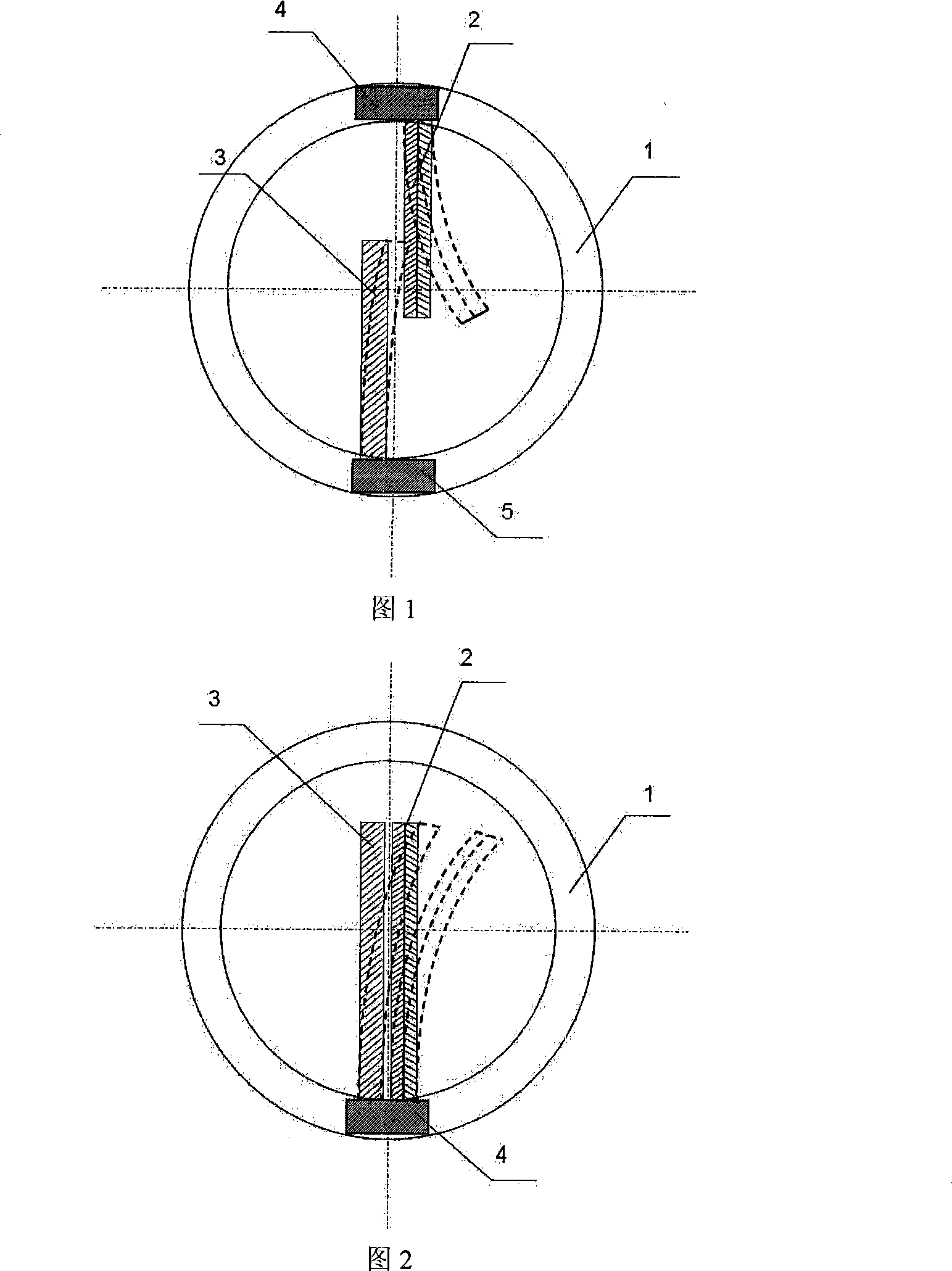
[0028] The carrying net includes a supporting part, a driving part and a mechanical testing part, the supporting part is a metal ring 1, and the driving part is a thermal bimetallic sheet 2 composed of different linear expansion coefficients and a metal sheet with a large linear expansion coefficient On the inner side, the metal sheet with a small coefficient of linear expansion is on the outside, and one end of the thermal bimetal sheet is fixed on the metal ring with a pressing piece 14, and the other end is a free end; On the other side, the cantilever beam 3, which is used to test the size of the force and has a known modulus of elasticity, is fixed on the metal ring using the compression piece II 5, and the slit width between the cantilever beam 3 and the thermal bimetal 2 is 2- 50 μm, distributed in the center of the metal ring 1 parallel to the thermal bimetal 2 and symmetrically.

[0029] The use steps of the present invention are as follows:

[0030]1. As shown in Fi...


PUM

PropertyMeasurementUnit
thicknessaaaaaaaaaa
widthaaaaaaaaaa
lengthaaaaaaaaaa

Abstract

A nanometer material stress test grid for a transmission electron microscope belongs to the field of nanometer material original position observation. The grid includes a supporting part, a drive part and a mechanical test part. The supporting part is a metal ring (1); the drive part is a thermal double-metal slice (2) formed by different linear expansibilities; one end of the drive part is fixed on the upper surface of the metal ring by a pressure bit I (4) and the other end is free; the other side of the metal ring utilizes a pressure bit II (5) to fix a suspension beam (3) with tested force and known elasticity modulus with the thermal double-metal slice in parallel, or the thermal double-metal slice and the suspension beam are arranged in parallel and are fixed on the same side of the metal ring by the pressure bit; all the clearance widths are 2 to 50 Mum and are symmetrically distributed on the center of a copper ring. The invention has the advantages of reliable performance, convenient mounting and simple structure can realize large angle tilting along the X and Y directions by utilizing a high resolution transmission electron microscope and acquire the stress dimension when acquiring a high resolution image of the microstructure change of nanometer material under stress action.

Description

technical field [0001] The invention relates to a device for testing the in-situ mechanical properties of nanometer materials in a transmission electron microscope. The device realizes the in-situ stretching of single-phase nanomaterials by heating the hot bimetallic sheet and drives the bending of the cantilever beam to realize the measurement of the mechanical properties of the nanomaterials, and the measurement of the electrical properties under the action of tensile stress. At the same time, the transmission electron microscope is used to observe the structure of nanomaterials in situ in real time while stretching, and the electrical conductivity characteristics before and after stretching deformation can be measured by external electrical signals, which belongs to the field of in situ observation of nanomaterials. Background technique [0002] Since the beginning of the 21st century, it can be said that people have made great progress in the research of nanomaterials, b...

Claims


Application Information

Patent Timeline
Patent Type & Authority Applications(China)
IPC IPC(8): G01N3/00G01N13/10H01J37/26G01Q30/20
Inventor 韩晓东岳永海郑坤张跃飞张泽
Owner BEIJING UNIV OF TECH
Why Eureka
Try Eureka