Method for detecting releasing degree of semiconductor chip from electrostatic chuck

An electrostatic chuck, semiconductor technology, used in semiconductor/solid-state device manufacturing, semiconductor/solid-state device testing/measurement, circuits, etc., can solve problems such as damage to the thimble and manipulator, wafer bounce or displacement, and lack of access to reduce accidents. Incidence, avoidance of jumping or shifting effects

Active Publication Date: 2008-07-16
BEIJING NAURA MICROELECTRONICS EQUIP CO LTD
View PDF0 Cites 7 Cited by
  • Summary
  • Abstract
  • Description
  • Claims
  • Application Information

AI Technical Summary

Problems solved by technology

[0004] But because the electrostatic chuck often cannot completely remove the electrostatic charge on the wafer and the electrostatic chuck when releasing the semiconductor wafer, in this case, there is still a residual attraction between the wafer and the electrostatic chuck. If the thimble is raised, it may cause the wafer to jump or shift, so that the manipulator cannot take the wafer, and even damage the thimble and the manipulator.
At present, there have been many studies on the method of releasing the wafer from the electrostatic chuck, but there is a lack of a method for judging the residual gravitational force between the wafer and the electrostatic chuck, that is, the method for judging the degree of wafer release. If the semiconductor wafer can be released from the electrostatic chuck By detecting the release degree of the semiconductor chip, the above-mentioned chip jumping or displacement can be avoided, the accident rate can be reduced, and the semiconductor chip can be safer and more reliable during the transmission process.

Method used


Image

  • Method for detecting releasing degree of semiconductor chip from electrostatic chuck
  • Method for detecting releasing degree of semiconductor chip from electrostatic chuck

Examples


Embodiment Construction

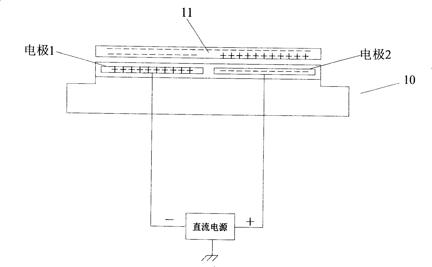
[0022] The invention provides a method for detecting the release degree of a semiconductor wafer from an electrostatic chuck. The core of the invention is: inject gas between the contact surface of the semiconductor wafer and the electrostatic chuck, and compare the detected gas leakage rate with the set The leakage rate threshold value is compared with the predetermined leakage rate, so as to judge the release degree of the semiconductor wafer according to the comparison result.

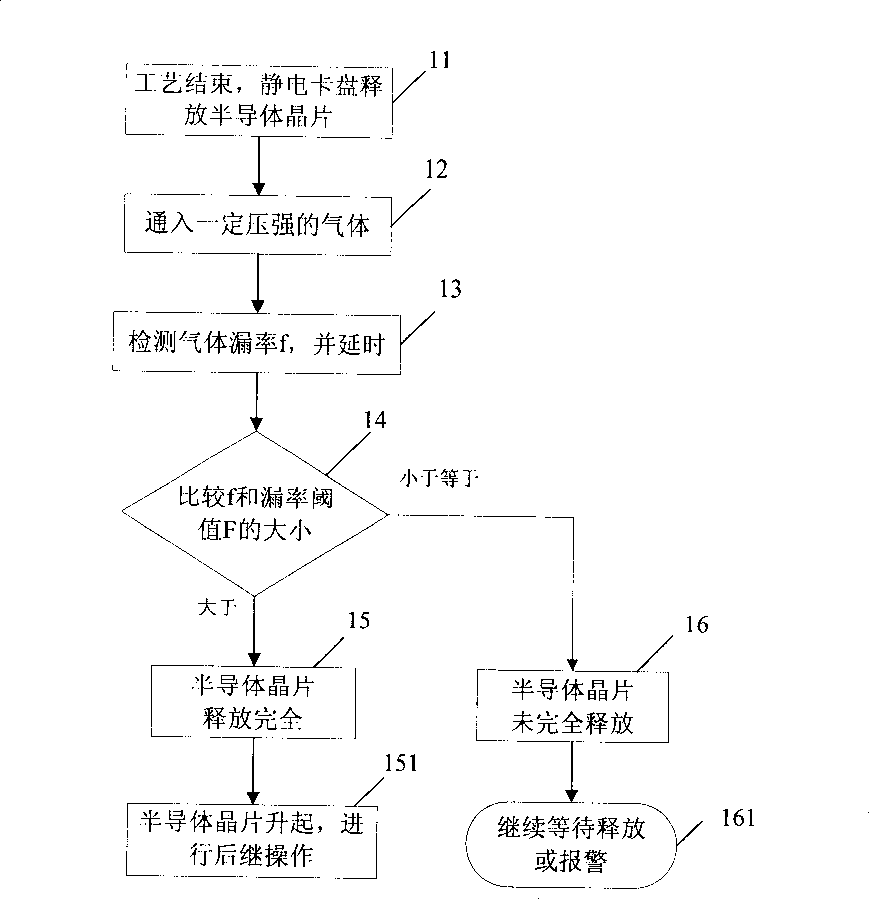
[0023] For better describing the present invention, now in conjunction with accompanying drawing, the method of the present invention is further described:

[0024] The operating process of the method of the present invention is as follows figure 2 As shown, the specific steps are,

[0025] Step 11: the process operation on the semiconductor wafer ends, and the electrostatic chuck releases the semiconductor wafer.

[0026] Step 12: Pass a gas between the contact surface of the semiconductor wafer...


PUM


Abstract

The invention provides a method for detecting the degree of the release of a semi-conductor chip from an electrostatic chuck, which in details comprises the following steps of: passing air between the semi-conductor chip and the electrostatic chuck and comparing the rate of the detected air leakage with the set threshold value of leakage rate so as to judge the degree of the release of the semi-conductor chip. With the detection method, the degree of the release of the semi-conductor chip from the electrostatic chuck can be judged effectively so as to conduct corresponding operation according to the degree of the release, which avoids the jump or displacement of the semi-conductor chip, reduces the accident rate and ensures the safety and reliability of the semi-conductor chip during transmission.

Description

technical field [0001] The invention relates to the field of semiconductor wafer production, in particular to a method for detecting the release degree of a semiconductor wafer from an electrostatic chuck. Background technique [0002] At present, in the production process of semiconductor wafers, in order to ensure the high quality of the wafers, automatic mechanical operations are used, including the processing, process packaging and transmission of semiconductor wafers. For example, in the transmission and processing of semiconductor wafers, mechanical chucks were generally used in earlier technologies to fix the wafers for semiconductor processing, but part of the wafer surface needed to be covered, which led to problems such as waste and high pollution. At present, electrostatic chucks are used instead. The chuck is used to transport, that is, the robot arm places the wafer on the electrostatic chuck in the reaction chamber, and the wafer is adsorbed on the electrostati...

Claims


Application Information

Patent Timeline
Patent Type & Authority Applications(China)
IPC IPC(8): H01L21/00H01L21/66
Inventor 刘利坚
Owner BEIJING NAURA MICROELECTRONICS EQUIP CO LTD
Why Eureka
Try Eureka