High speed gallium arsenide based channel strain high electron mobility transistor material

A high electron mobility, compound channel technology, applied in the field of compound semiconductor materials, can solve the problems of fragile InP substrate, restricting power amplifier circuits, low source-drain breakdown voltage, etc., and achieves superior millimeter-wave frequency device characteristics, Superior millimeter-wave frequency characteristics and the effect of improving the source-drain breakdown voltage

Active Publication Date: 2008-07-16
北京中科微投资管理有限责任公司
View PDF0 Cites 5 Cited by
  • Summary
  • Abstract
  • Description
  • Claims
  • Application Information

AI Technical Summary

Problems solved by technology

[0003] GaAs-based HEMTs are mainly used below the Ka band, while InP-based HEMTs still have high gain and low noise performance in the higher W-band, but the shortcomings of InP-based HEMTs are: first, the source-drain breakdown voltage is low, and the output power Small, which restricts its application in microwave power amplifier circuits; second, the InP substrate is fragile, the chip size is ...

Method used


Image

  • High speed gallium arsenide based channel strain high electron mobility transistor material
  • High speed gallium arsenide based channel strain high electron mobility transistor material
  • High speed gallium arsenide based channel strain high electron mobility transistor material

Examples


Embodiment Construction

[0029] In order to make the objectives, technical solutions, and advantages of the present invention clearer, the following further describes the present invention in detail in conjunction with specific embodiments and with reference to the accompanying drawings.

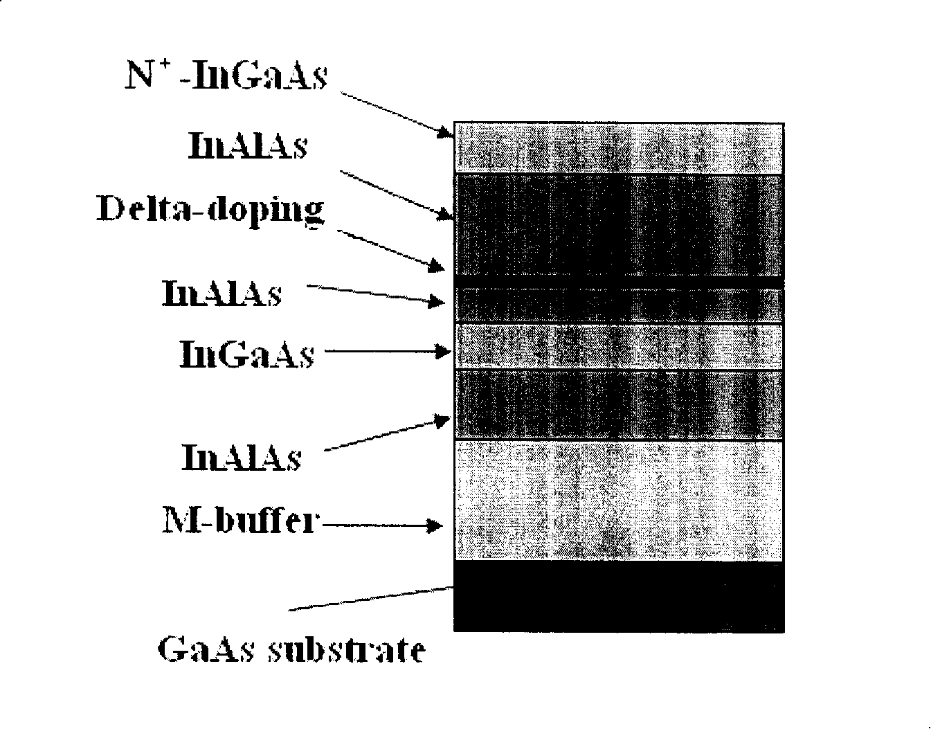
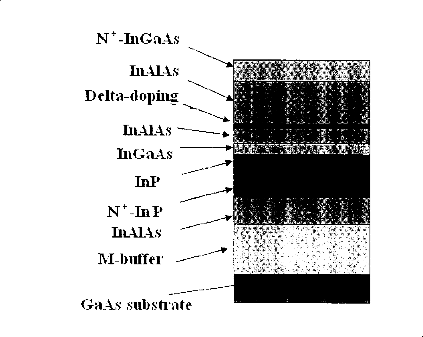
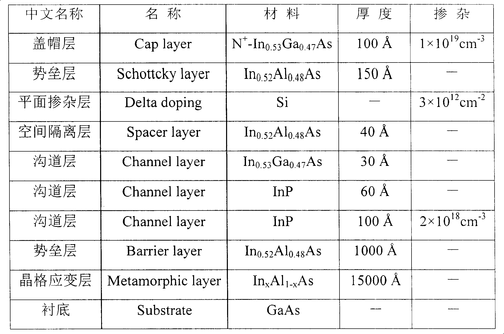
[0030] Such as figure 2 As shown, figure 2 It is a schematic diagram of the high-speed gallium arsenide-based composite channel MHEMT material provided by the present invention. The MHEMT material is composed of a lattice strain layer In which is sequentially epitaxially grown on a GaAs substrate. x Al 1-x As, barrier layer under the channel In0.52 Al 0.48 As, channel layer doped with InP, channel layer without InP, channel layer with In 0.53 Ga 0.47 As, space isolation layer In 0.52 Al 0.48 As, planar doped layer, barrier layer In 0.52 Al 0.48 As and highly doped cap layer In 0.53 Ga 0.47 As composition.

[0031] Among them, the lattice strain layer In x Al 1-x As is grown on GaAs substrate by low-temperature epitaxial...


PUM


Abstract

The invention relates to the compound semi-conductor material technical field and discloses a high-speed GaAs-based composite channel MHEMT material. The MHEMT material consists of a lattice strain layer InAl<1-x>As, a channel lower barrier layer In0.52AL0.48As, a channel layer doped with InP, a channel layer without InP, a channel layer In0.53Ga0.47As, a space separation layer In0.52Al0.48As, a planar doping layer, a barrier layer In0.52Al0.48As and a highly-doped GaAs cap layer In0.53Ga0.47As which are in orderly epitaxial growth on a GaAs substrate. The invention combines the characteristics that the In0.53Ga0.47As has high electron mobility in low field, and the InP has high threshold energy and high saturation rate in high field, solves the disadvantage that a routine MHEMT device has low source/drain breakdown voltage, achieves the intentions of improving the source/drain breakdown voltage and ensuring that the device has excellent millimeter wave frequency characteristic.

Description

Technical field [0001] The invention relates to the technical field of compound semiconductor materials, in particular to a high-speed gallium arsenide-based composite channel strained high electron mobility transistor material. Background technique [0002] High Electron Mobility Transistor (HEMT) has the characteristics of high frequency, high speed, high power gain and low noise figure, so it is widely used in military, space and civil communication fields. Such as millimeter wave radar, electronic warfare, intelligent equipment, satellite communications and radiation astronomy. [0003] GaAs-based HEMTs are mainly used below the Ka band, while InP-based HEMTs still have high gain and low noise performance at higher W-bands, but the disadvantages of InP-based HEMTs are: First, the source-drain breakdown voltage is low, and the output power Small, restricting its application in microwave power amplifier circuits; second, the InP substrate is fragile, the chip size is small, the...

Claims


Application Information

Patent Timeline
IPC IPC(8): H01L29/778H01L29/201
Inventor 徐静波张海英叶甜春尹军舰
Owner 北京中科微投资管理有限责任公司
Why Eureka
Try Eureka