Method for reducing ion implantation damage influence of mercury cadmium telluride photovoltaic device

An ion implantation, photovoltaic device technology, applied in semiconductor devices, electrical components, sustainable manufacturing/processing, etc., can solve problems such as weak inversion, and achieve the effect of improving device performance and avoiding inversion

Inactive Publication Date: 2008-07-23
SHANGHAI INST OF TECHNICAL PHYSICS - CHINESE ACAD OF SCI
View PDF0 Cites 9 Cited by
  • Summary
  • Abstract
  • Description
  • Claims
  • Application Information

AI Technical Summary

Problems solved by technology

[0003] The purpose of the present invention is to provide a method for reducing the impact of ion implantation damage on mercury cadmium telluride photovoltaic devices, and to solve the problem of P-type regions th

Method used


Image

  • Method for reducing ion implantation damage influence of mercury cadmium telluride photovoltaic device
  • Method for reducing ion implantation damage influence of mercury cadmium telluride photovoltaic device

Examples


Embodiment Construction

[0020] The specific embodiment of the present invention is described in further detail below in conjunction with accompanying drawing:

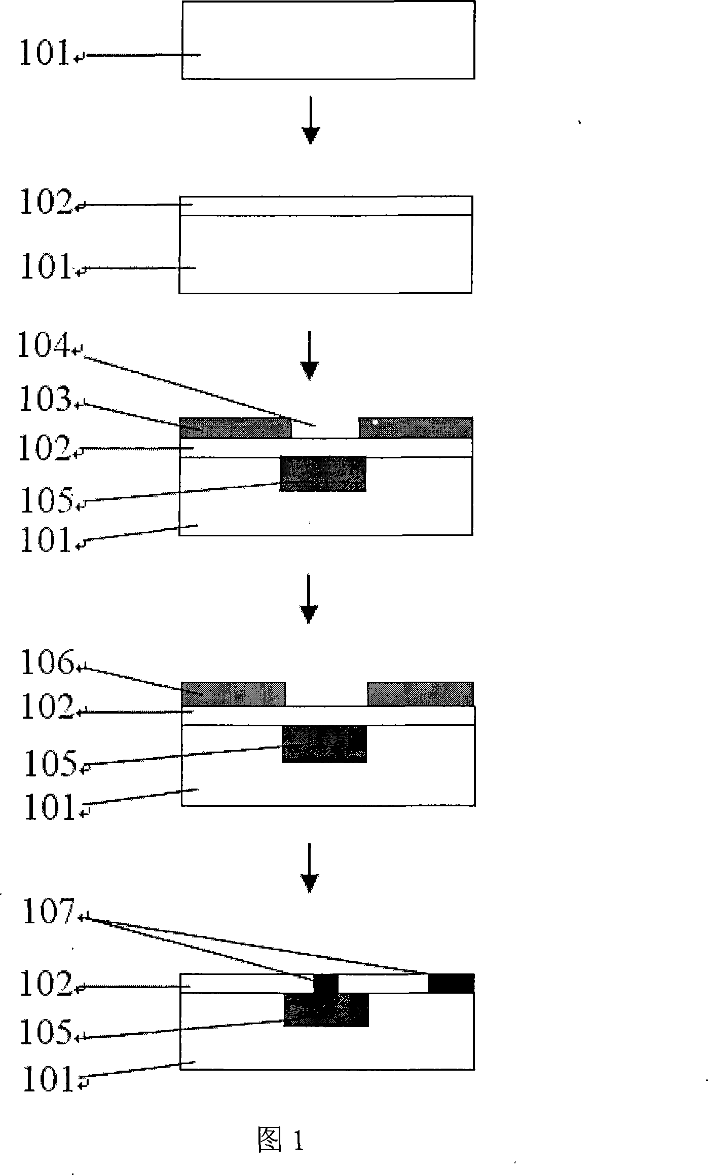
[0021] Figure 1 shows the preparation process of planar photovoltaic devices. After conventional cleaning and etching processes are performed on the P-type HgCdTe substrate 101, a layer of ZnS 102 with a thickness of 100nm is grown on the surface as a barrier layer for the ion implantation process. Use photoresist 103 for protection, and then perform B + Ion implantation, the implantation energy is 140KeV, and the implantation dose is 10 14 cm -2 . Inject B + The ions form an N-type inversion region 105 on the P-type HgCdTe material, thereby forming a PN junction. It should be pointed out that due to the diffusion of implanted ions in the horizontal direction, the actually formed N-type inversion region 105 is larger than the implanted region 104 defined by photolithography; after implantation, the photoresist on the surface of the sampl...


PUM


Abstract

The invention discloses a method for reducing the effects of ion radiation damage of a mercury cadmium telluride photovoltaic device. The method is that a mercury cadmium telluride sample after being injected with ions are defined into a hydrogen ion treatment region through lithography, and then the sample is put in an atmosphere of hydrogen ion to treat. The hydrogen ion treatment region is determined through a method of changing the area, form the size of an initial defined ion implanted region, the hydrogen ion treatment region is gradually enlarged, the current-voltage curve of the mercury cadmium telluride sample which is treated through the hydrogen in different regions is tested, and the size of the hydrogen ion treatment region is determined through observing the increasing phenomenon of a dark current under a reverse bias.

Description

technical field [0001] The invention relates to an infrared semiconductor device manufacturing technology, in particular to a method for reducing the impact of ion implantation damage on mercury cadmium telluride (HgCdTe) photovoltaic devices, which is used in the ion implantation process of planar mercury cadmium telluride photovoltaic devices. Background technique [0002] There are two types of HgCdTe infrared detectors: photoconductive and photovoltaic. At present, the application of photovoltaic devices is the main direction. The core of photovoltaic devices is the PN junction, and the formation methods of the PN junction include diffusion and ion implantation, among which ion implantation has been widely used due to its advantages of simple process, strong controllability and room temperature implantation. The ion implantation process is to perform selective area implantation on the surface of the P (or N) type material, so that the implanted area is reversed to form a...

Claims


Application Information

Patent Timeline
IPC IPC(8): H01L31/18
CPCY02P70/50
Inventor 乔辉周文洪叶振华蒋科贾嘉李向阳
Owner SHANGHAI INST OF TECHNICAL PHYSICS - CHINESE ACAD OF SCI
Why Eureka
Try Eureka