Flexible substrate integrated waveguides

A substrate-integrated waveguide and substrate technology, applied in waveguides, waveguide-type devices, antennas, etc.

Inactive Publication Date: 2008-07-23
SONY DEUT GMBH
View PDF0 Cites 14 Cited by
  • Summary
  • Abstract
  • Description
  • Claims
  • Application Information

AI Technical Summary

Problems solved by technology

Also, manufacturing should be easier, but should still allow complex structural components

Method used


Image

  • Flexible substrate integrated waveguides
  • Flexible substrate integrated waveguides

Examples


Embodiment Construction

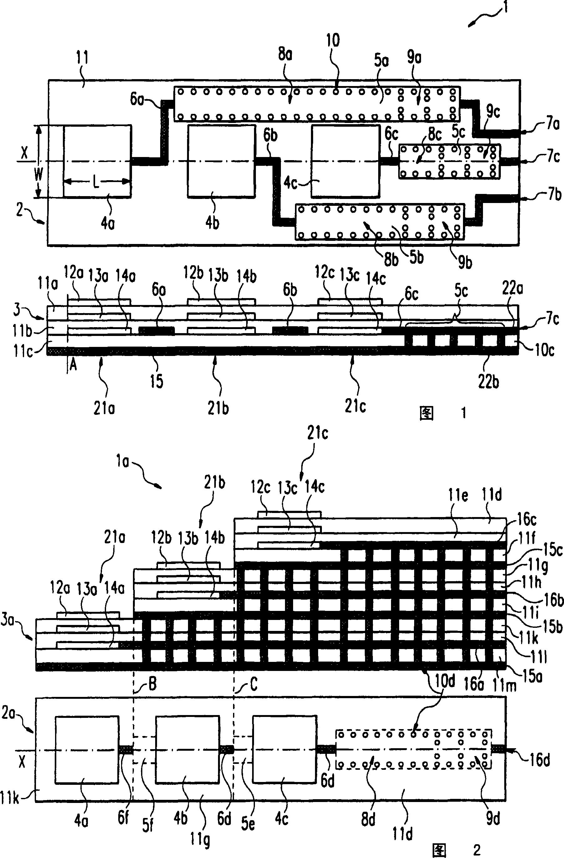
[0031] Figure 1 shows a substrate structure 1 comprising its top view 2 and its cross section 3.

[0032] Top view 2, the top view allows to see the parts partially below the surface, the surface includes the top layer 11a, the top view shows the first planar antenna 4a, the second planar antenna 4b, the third planar antenna 4c, The corresponding microstrip lines 6a, 6b, 6c, the corresponding substrate integrated waveguides (SIWG) 5a, 5b, 5c and the corresponding feed lines 7a, 7b, 7c are all partly / integrated on or in the substrate 11. All the above-mentioned components are located on the same substrate / component, so they can be subsequently and / or gradually fabricated on the same wafer or semiconductor substrate or LCP (liquid crystal polymer) substrate or any other material suitable for stacking the substrate structure 1 on.

[0033] The planar antennas 4a, 4b, 4c are arranged in a row, and are symmetrical along the symmetry axis X, are equidistant from each other, and are shap...


PUM


Abstract

This invention relates to a device operable to guide electromagnetic waves in substrate integrated structures, said substrate integrated structures being made in one component. In detail planar antennas are part of said substrate integrated structures, which are connected to electromagnetic waveguides. This invention also allows 3D structures of the above mentioned components in a multilayer substrate.

Description

Technical field [0001] The present invention relates to the field of substrate integrated structures, in particular to substrate integrated waveguides. Especially for high-frequency signals, a substrate integrated waveguide is necessary. Background technique [0002] problem [0003] The current communication system has proved to be rapidly developing towards system integration and miniaturization. Antennas and channel filters are key components in these communication systems, and the selection criteria for successful communication include, among other things, the performance, size, weight, and cost of the antenna. [0004] A multi-beam antenna system employing a beam switching mechanism for different antenna units requires a relatively large space in order to connect the antenna units to system components. These feeders suffer from high losses and poor matching, especially for long feeders in the millimeter wave frequency region. In addition, there is low insulation between thes...

Claims


Application Information

Patent Timeline
Patent Type & Authority Applications(China)
IPC IPC(8): H05K1/02H05K3/46H01P3/08H01P1/20H01Q13/08
CPCH01Q21/065H01Q21/0075
Inventor S·科克M·艾-蒂克里蒂
Owner SONY DEUT GMBH
Why Eureka
Try Eureka