
Eureka
For R&D, Eureka makes reading and utilizing patents & technical documents easy.
Eureka AIR
Designed for self-driven R&D workflows. Generate viable solutions, solve complex R&D challenges, empower your innovation with AI.

Eureka Materials
Designed for material experts only. Revolutionize your material R&D, from search, analyze, to developing new materials.

TechResearch
Generate reliable direction feasibility study reports for your R&D in just a few steps.

TechSeek
Discover and master advanced knowledge NOW. Basics, ideas, possibilities, all at once.

TechMind
As an expert in R&D Theories, TechMind can generates customized viable solutions instantly.

TechRisk
Analyze your overall solution with one click, know your potential R&D risks in advance.

TechMonitor
Get weekly tech updates, stay abreast of the latest tech innovations and key insights.
Current or voltage measuring circuit, sense circuit, nonvolatile semiconductor memory, and differential amplifier
The technology of a voltage measurement circuit and a differential amplifier, which is applied in another field, can solve the problems of an increase in the number of storage cells, electrical imbalance, mixed with differential noise, etc., and achieve the effect of strong noise resistance and high precision
- Summary
- Abstract
- Description
- Claims
- Application Information
AI Technical Summary
Problems solved by technology
Method used
Image

Examples
Embodiment 1
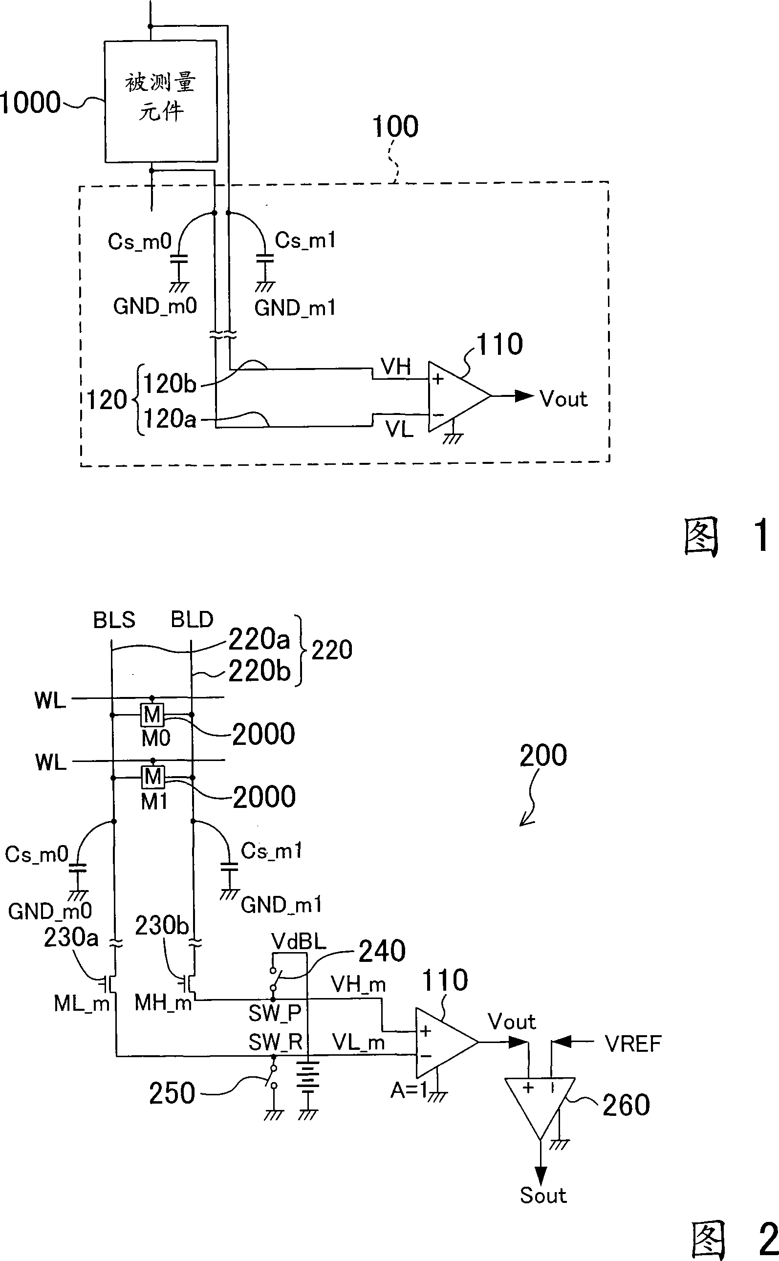
FIG. 1 is a block diagram showing the structure of a voltage difference measurement circuit 100 according to Embodiment 1 of the present invention. The voltage difference measurement circuit 100 measures the voltage difference between the two output terminals of the device under test 1000 by differentially amplifying the voltage between the two output terminals.
[0048] Specifically, the voltage difference measurement circuit 100 as shown in FIG. 1 includes a differential amplifier 110 and a pair of wirings 120 .
[0049] The differential amplifier 110 amplifies the voltage difference of the input signal and outputs it. In this embodiment, the gain (A) of the differential amplifier 110 is set to 1. In addition, a node (node) to which a positive phase (high side) voltage of the differential amplifier 110 is input is referred to as VH, and a node to which a negative phase (negative phase) side (low side) voltage is input is referred to as VH. for VL.
[0050] The pair of wiri...
Embodiment 2
FIG. 2 is a block diagram showing the structure of a readout circuit 200 according to Embodiment 2 of the present invention. The readout circuit 200 is an example in which the voltage difference measurement circuit 100 involved in the first embodiment is applied to a readout circuit in a storage circuit.
[0062] The read circuit 200 reads information stored in the memory cell 2000 (M0, M1 in FIG. 2). This memory cell 2000 is a nonvolatile memory in which a cell current of a read cell changes according to written information. In this embodiment, for convenience of description, it is assumed that a prescribed read current flows when "1" is stored as information, and that current does not flow when "0" is stored as information.
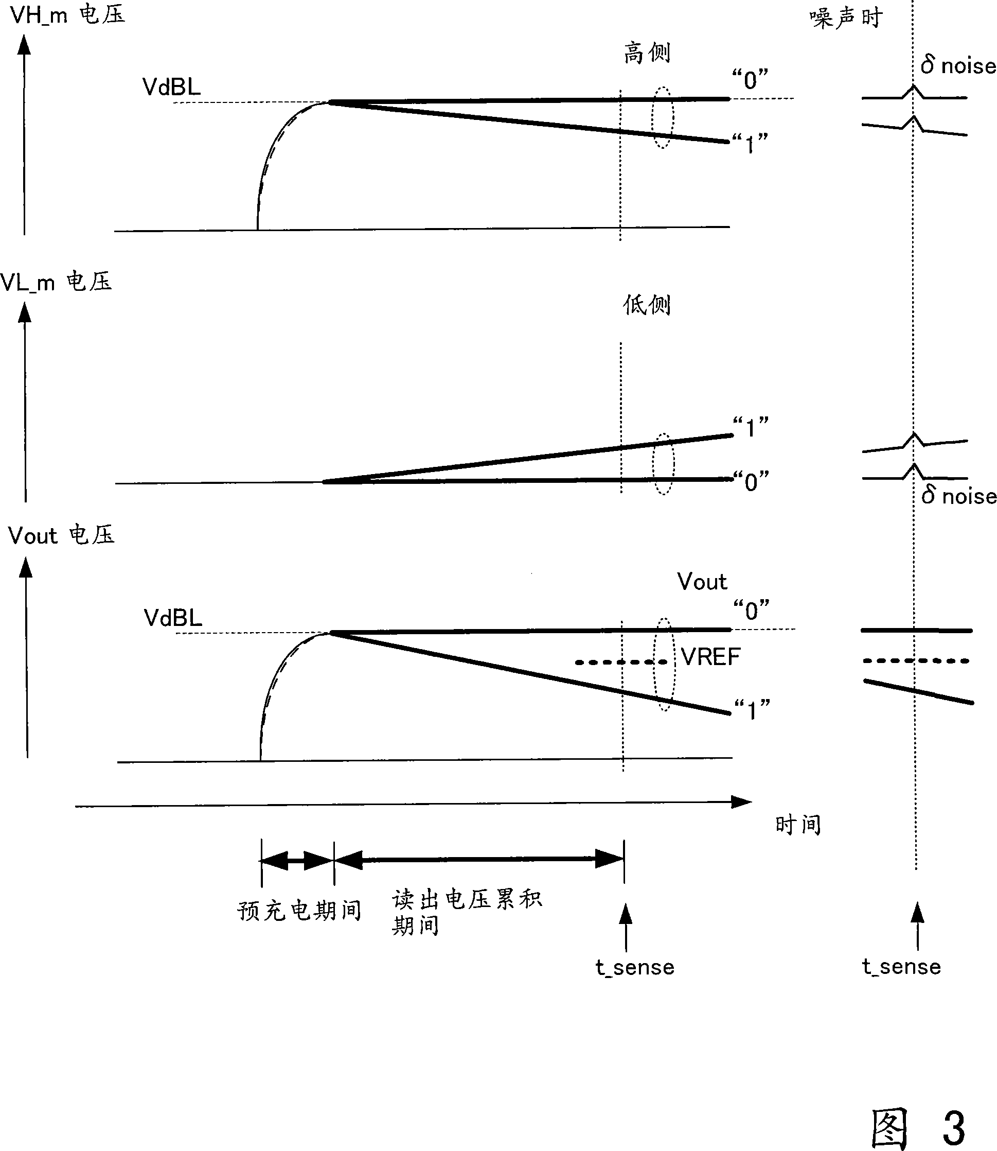
[0063] As shown in FIG. 2 , readout circuit 200 is configured to include differential amplifier 110 , a pair of wiring lines 220 , selection transistors 230 a and 230 b , precharge switch 240 , reset switch 250 , and differential amplifier 260 . In add...
Embodiment 3
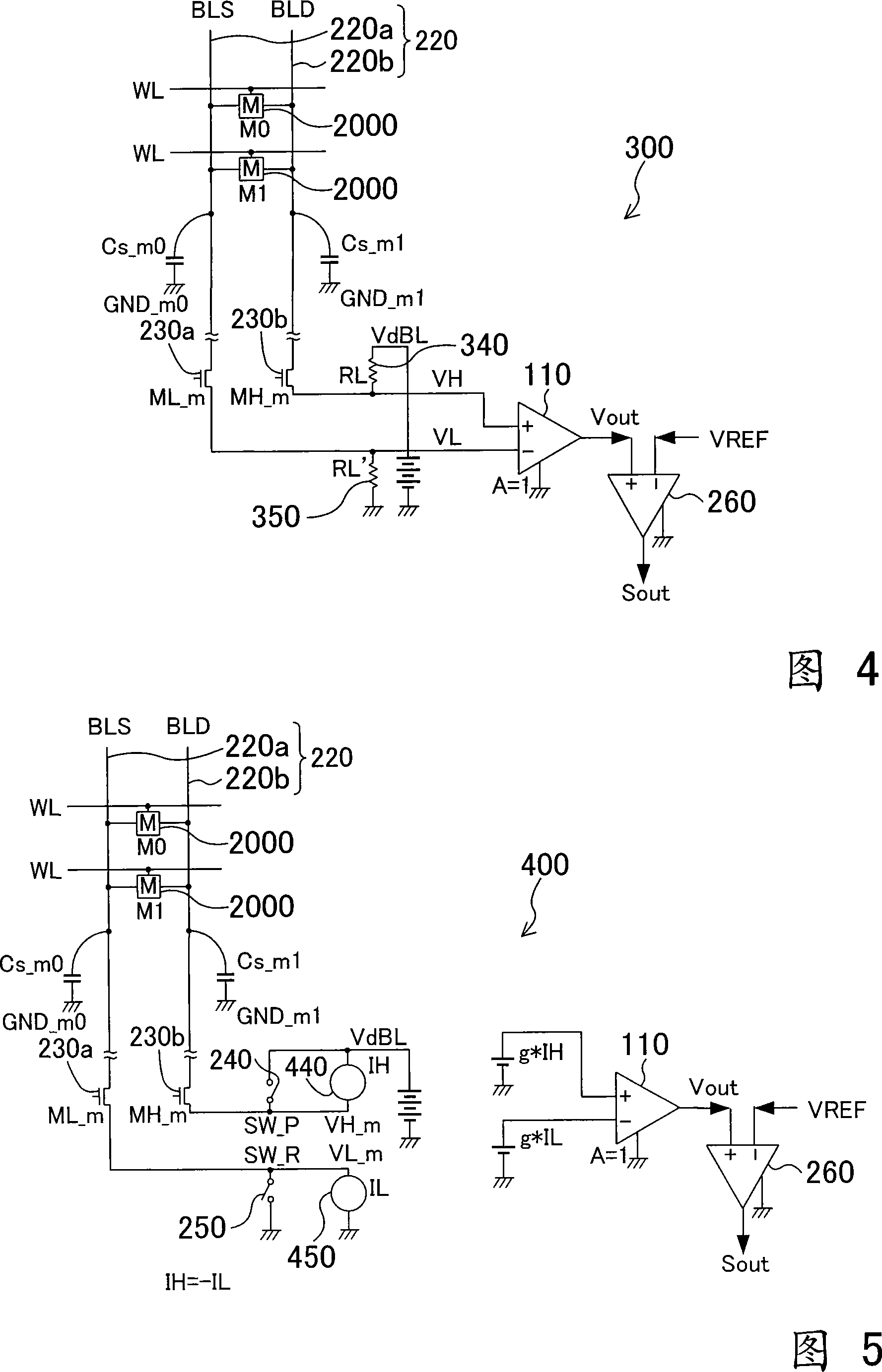
FIG. 4 is a block diagram showing the structure of a readout circuit 300 according to Embodiment 3 of the present invention. As shown in FIG. 4 , the readout circuit 300 includes a pull-up resistor 340 (RL) and a pull-down resistor 350 (RL′). The pull-up resistor 340 (RL) replaces the precharge switch 240 in Embodiment 2, and the pull-down resistor 350 (RL′) replaces the reset switch 250 . In the readout circuit 200 involved in the second embodiment, the state of the memory cell is judged through dynamic operation, and in this embodiment, the state of the memory cell is judged according to whether there is a state of "0" or "1" in the memory cell current to read data.
[0078] In the readout circuit 300 configured as described above, when information is read from the memory cell 2000 , a voltage drop and a voltage rise occur in the pull-up resistor 340 and the pull-down resistor 350 . As a result, the voltages of the high-side and low-side nodes of the differential amplifier ...
PUM
 Abstract
Description
Claims
Application Information
 - R&D Engineer
- R&D Manager
- IP Professional
- Industry Leading Data Capabilities
- Powerful AI technology
- Patent DNA Extraction
Browse by: Latest US Patents, China's latest patents, Technical Efficacy Thesaurus, Application Domain, Technology Topic, Popular Technical Reports.
© 2024 PatSnap. All rights reserved.Legal|Privacy policy|Modern Slavery Act Transparency Statement|Sitemap|About US| Contact US: help@patsnap.com