Method for thinning a sample and sample carrier for performing the method

A sample and carrier technology, used in semiconductor/solid-state device manufacturing, discharge tubes, electrical components, etc., to solve problems such as hindering the automation of thinning processes

Inactive Publication Date: 2008-08-13
FEI CO
View PDF0 Cites 10 Cited by
  • Summary
  • Abstract
  • Description
  • Claims
  • Application Information

AI Technical Summary

Problems solved by technology

This hinders the automation of the thinning process

Method used


Image

  • Method for thinning a sample and sample carrier for performing the method
  • Method for thinning a sample and sample carrier for performing the method

Examples


Embodiment Construction

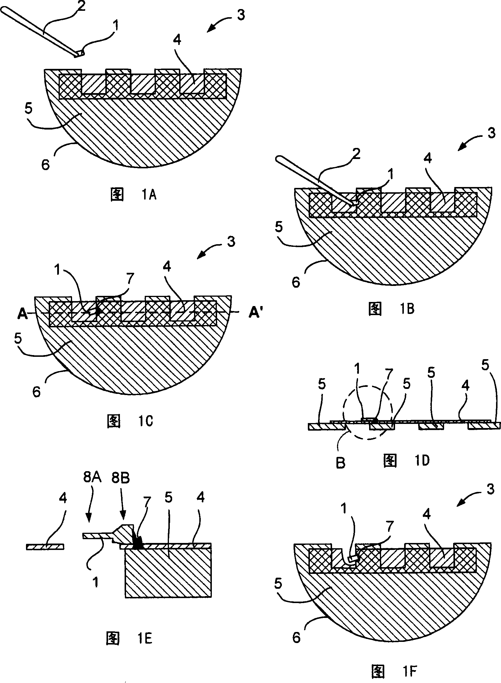
[0052] Figure 1A schematically depicts a sample carrier according to the invention and a probe carrying a sample approaching the sample carrier.

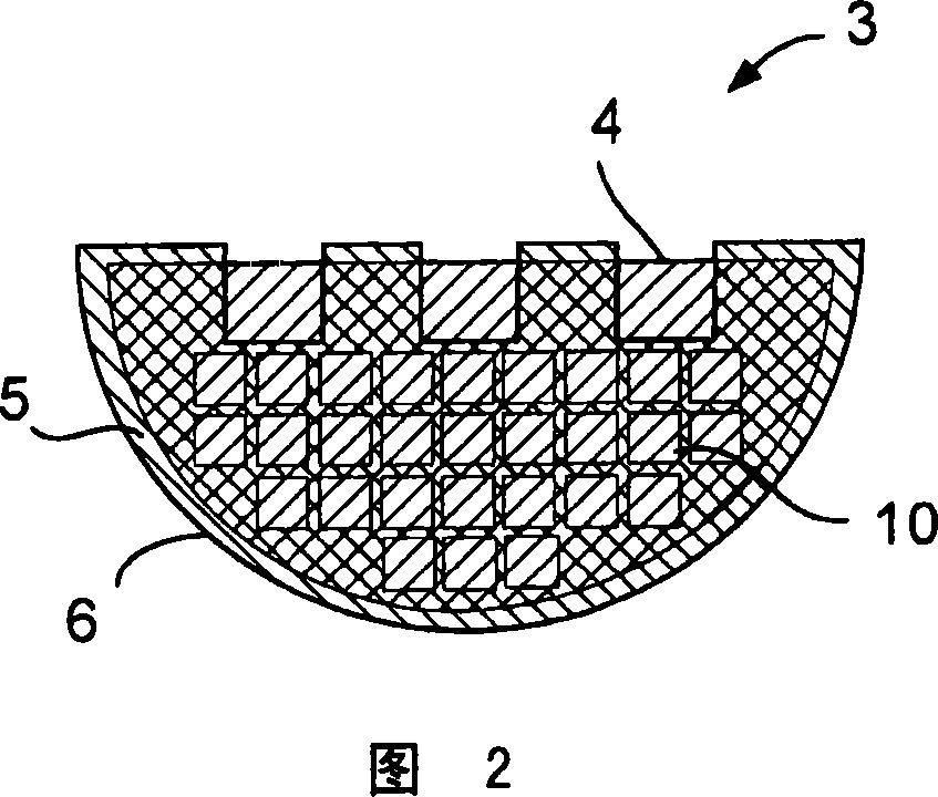
[0053] FIG. 1A shows a sample 1 attached to a probe 2 . The sample carrier 3 consists of two parts, a support membrane 4 and a rigid structure 5 . The rigid structure exhibits an outer boundary6. The supporting membrane extends partially beyond this outer boundary 6 of the rigid structure 5 .

[0054] The rigid structure of the sample carrier can be copper foil. Other materials, preferably electrically conductive materials, can likewise be used. Likewise, the support film is preferably electrically conductive, such as a carbon film or a conductive polymer film. However, support films made of silicon or, for example, nitride are also conceivable.

[0055] The sample 1 may be attached to the probe 2 by electrostatic forces, for example to a probe in the form of a charged glass electrode. Other attachment means can also be used, ...


PUM


Abstract

The invention describes a sample carrier (3) for thinning a sample (1) taken from eg a semiconductor wafer. The sample carrier comprises a rigid part (5), eg made of copper, with an outer boundary (6) and a support membrane (4), eg made of carbon, extending beyond said outer boundary. By placing the sample on a support membrane, for example IBID can be used to attach the sample to a rigid structure. The support film aligns the sample when the sample is placed on the support film. After attaching the sample to the rigid structure, the sample can be thinned, for example with an ion beam, during which the support membrane is also locally removed. The invention achieves a better alignment of the sample to the sample carrier and more freedom in how the sample is transferred from the wafer to the sample carrier by means of eg a charged glass needle (2). The latter eliminates the attachment / detachment steps normally associated with transferring the sample to the sample carrier.

Description

technical field [0001] The present invention relates to a method for thinning a sample comprising: [0002] provide the sample attached to the probe, [0003] providing a sample carrier exhibiting a rigid structure presenting boundaries to which the sample can be attached, [0004] · attaching the sample to the boundary of the rigid structure, and [0005] - exposing the sample to a milling or etching treatment in order to at least partially thin the sample. [0006] The invention also relates to a sample carrier for carrying out the method according to the invention. Background technique [0007] This method is described in the article "The total release method for FIB in-situ TEM sample preparation" by T.M.Moore in Microscopy Today, Vol.13, No.4, pages 40-42, more specifically page 40, page 2 Column "The total release method for in-situ lift-out". [0008] This method is used eg in the semiconductor industry where samples are taken from semiconductors for inspection / a...

Claims


Application Information

Patent Timeline
Patent Type & Authority Applications(China)
IPC IPC(8): H01L21/00H01L21/683
CPCH01J37/20H01J37/3056H01J2237/31745
Inventor R·莱曼
Owner FEI CO
Why Eureka
Try Eureka