Nonvolatile semiconductor memory device
A storage device, non-volatile technology, applied in the direction of semiconductor devices, electric solid-state devices, electrical components, etc., can solve problems such as unstable operation
- Summary
- Abstract
- Description
- Claims
- Application Information
AI Technical Summary
Problems solved by technology
Method used
Image

Examples
no. 1 Embodiment approach
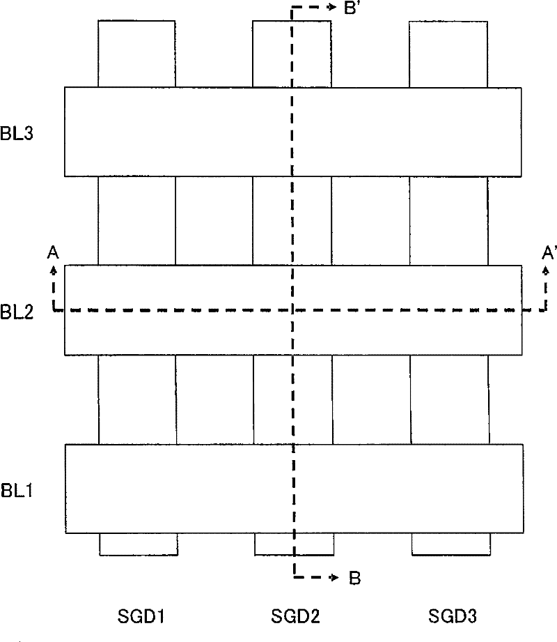
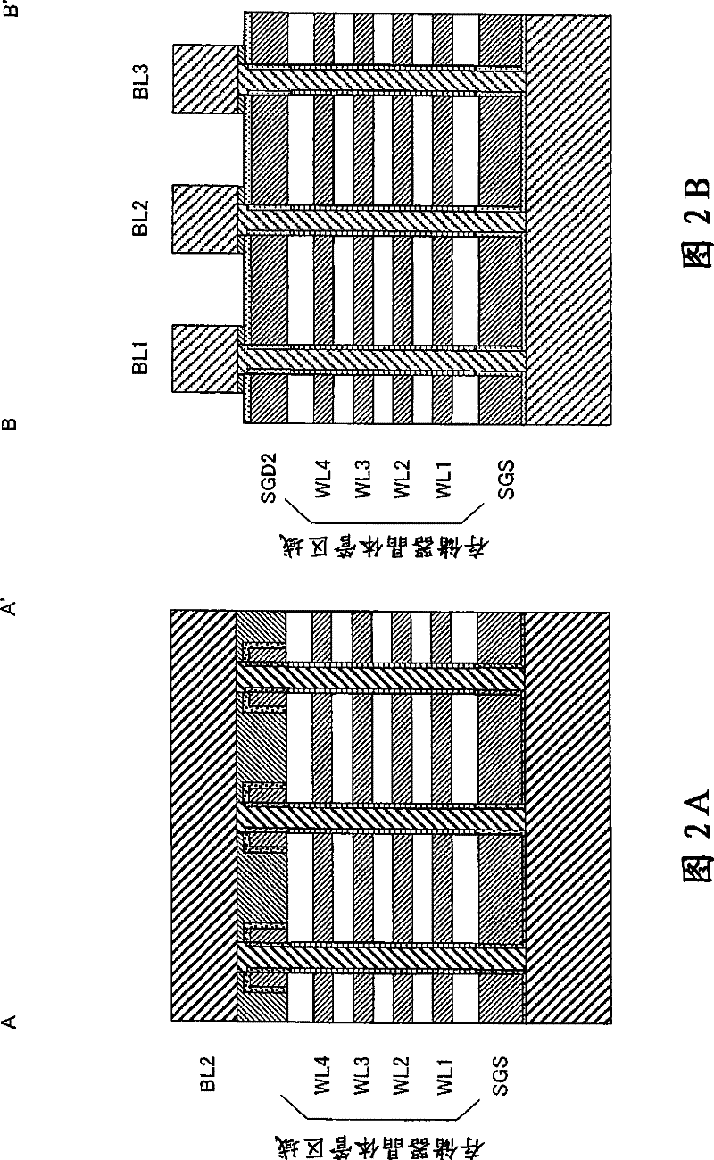
[0034] figure 1 It is a plan view of the nonvolatile semiconductor memory device according to the first embodiment seen from above. exist figure 1 In the nonvolatile semiconductor storage device, a plurality of bit lines BL1 to BL3 and a plurality of drain side select gate transistors SGD1 to SGD3 are arranged in an array. Figure 2A yes figure 1 The A-A' line sectional view of the nonvolatile semiconductor memory device, Figure 2B yes figure 1 The B-B' line sectional view of the nonvolatile semiconductor memory device.
[0035] exist Figure 2A with Figure 2B Among them, in the memory transistor region of the nonvolatile semiconductor memory device according to the first embodiment of the present invention, the memory cells are stacked and formed on the substrate by forming the semiconductor layer into a columnar shape. exist Figure 2A with Figure 2B In the memory transistor region shown in , a case where 4 layers of memory cells are stacked is shown. In additio...
no. 2 Embodiment approach
[0084] In the nonvolatile semiconductor memory device according to the second embodiment of the present invention, the structure formed by stacking the memory cells on the substrate by forming the semiconductor layer in the memory transistor region into a columnar shape is the same as that in the first embodiment. The difference is that instead of using a single semiconductor material, a cylindrical semiconductor that is the active layer constituting the memory transistor is formed with mutually different semiconductor materials on the edge portion (the portion on the gate side) and the central portion of the cylindrical cross section. area. Also, the semiconductor in the central portion of the cylinder employs a material whose valence electron band is closer to the vacuum level than the valence electron band of the semiconductor in the peripheral portion of the cylinder.
[0085] Figure 29 It is a diagram showing the general structure of the memory transistor region of the ...
no. 3 Embodiment approach
[0109] In the above-mentioned second embodiment, a case was shown in which the Si layer at the edge of the cylindrical semiconductor region serving as the active layer and the SiGe layer at the center were formed in two layers. In this third embodiment, refer to Figure 46 with Figure 47 A case where the molar ratio of Ge is gradually changed in forming the active layer so that the valence electron band is gradually changed from the edge to the center will be described.
[0110] Figure 46 It is a diagram schematically showing a state in which the Ge molar ratio of SiGe gas is gradually changed when forming a columnar semiconductor region as an active layer as time elapses from the edge portion to the center portion. In this figure, the Ge molar ratio of SiGe gas gradually changes when the central part of the cylinder is formed over time, and finally becomes SiGe gas. 0.7 Ge 0.3 example, but can also be changed for example to Si 0.9 Ge 0.1 ~ Si 0.7 Ge 0.3 . In the th...
PUM
 Abstract
Description
Claims
Application Information
 - R&D
- Intellectual Property
- Life Sciences
- Materials
- Tech Scout
- Unparalleled Data Quality
- Higher Quality Content
- 60% Fewer Hallucinations
Browse by: Latest US Patents, China's latest patents, Technical Efficacy Thesaurus, Application Domain, Technology Topic, Popular Technical Reports.
© 2025 PatSnap. All rights reserved.Legal|Privacy policy|Modern Slavery Act Transparency Statement|Sitemap|About US| Contact US: help@patsnap.com