

Semiconductor switch
A semiconductor and switch technology, applied in the field of semiconductor switches, can solve the problems of increased leakage current and increased chip cost, and achieve the effect of preventing leakage current and high-speed operation output voltage accuracy
- Summary
- Abstract
- Description
- Claims
- Application Information
AI Technical Summary
Problems solved by technology
Method used
Image

Examples
no. 1 Embodiment approach
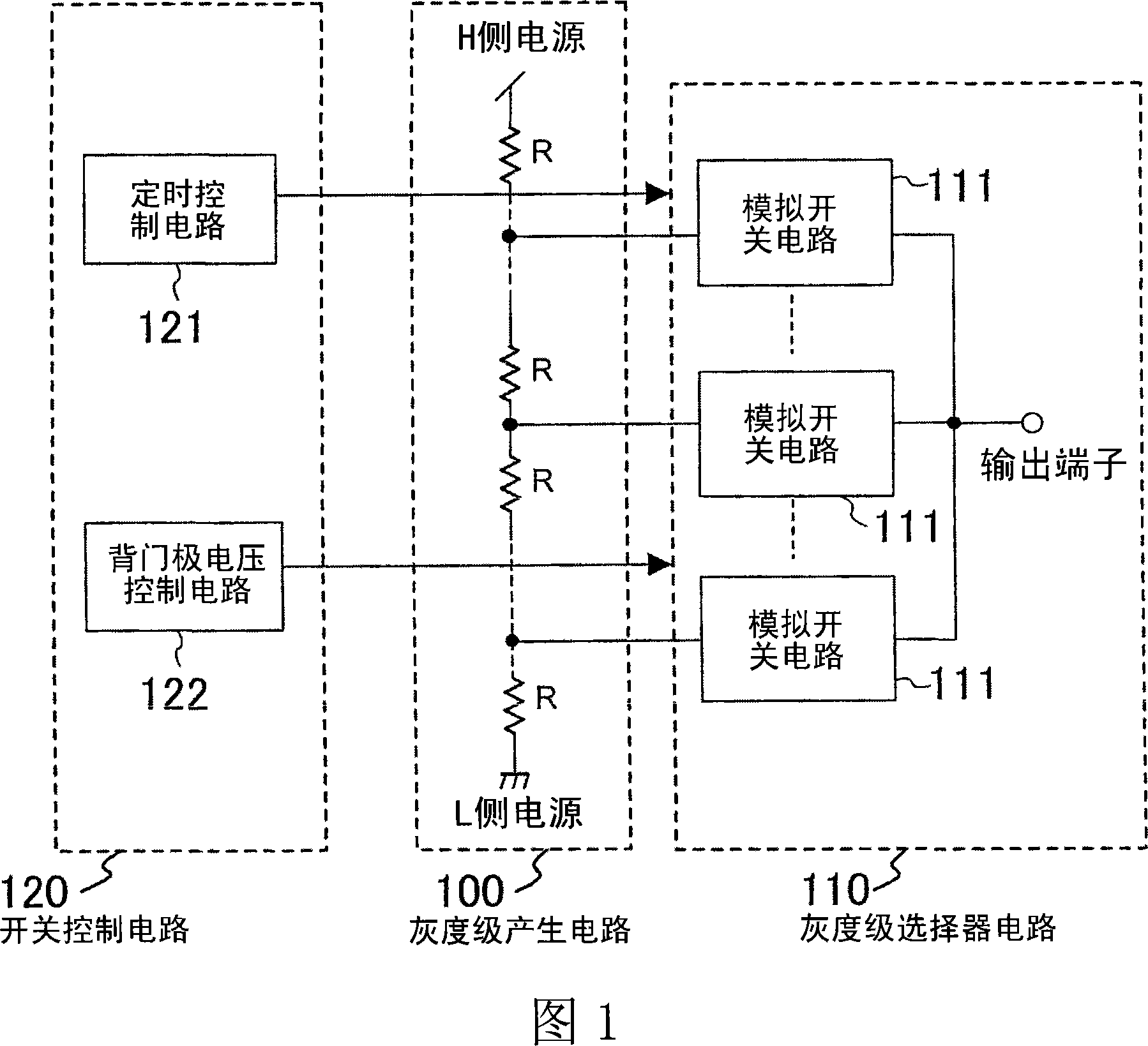
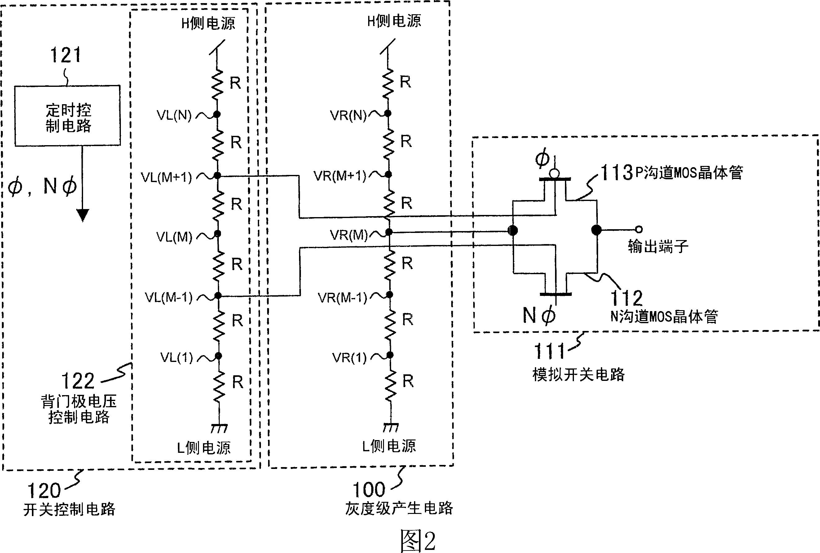
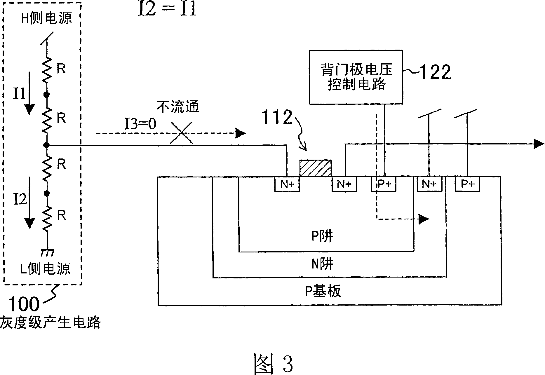
[0045] A semiconductor switch according to a first embodiment of the present invention will be described with reference to FIGS. 1 and 2 . The semiconductor switch according to the first embodiment of the present invention is composed of a grayscale generation circuit 100 , a grayscale selector circuit 110 , and a switch control circuit 120 , and the switch control circuit 120 is composed of a timing control circuit 121 and a backgate voltage control circuit 122 .
[0046]Among them, the grayscale generation circuit 100 is composed of a resistor string circuit in which a plurality of resistor elements R are connected in series between the H-side power supply and the L-side power supply. The number of resistive elements R is N, and the number of grayscale voltages generated at the connection points between the resistors is N−1. The voltages of the H-side power supply and the L-side power supply, and the size and number of the resistance elements R are determined by design based...
no. 2 Embodiment approach 》
[0054] A semiconductor switch according to a second embodiment of the present invention will be described with reference to FIG. 4 . The semiconductor switch of the second embodiment is composed of an analog switch circuit 211 , a switch control circuit 220 , and a gray scale generation circuit 200 . In addition, the switch control circuit 220 is composed of a timing control circuit 121 , a back gate voltage control circuit 222 and a bias circuit 223 .
[0055] Here, since the timing control circuit 121 has the same configuration as that of the first embodiment, the same components as those in FIGS. 1 and 2 are assigned the same symbols, and detailed description thereof will be omitted.
[0056] The grayscale generation circuit 200 has a structure in which a P-channel MOS transistor M2, a plurality of resistance elements R, and a diode D0 are connected in series between an H-side power supply and an L-side power supply. In addition, the back gate voltage control circuit 222 h...
PUM
 Abstract
Description
Claims
Application Information